


















Lesson 41 of 45 · Projects and Practice
Project: design and simulate a buck converter
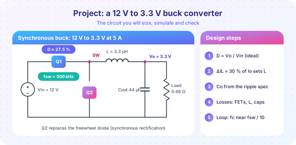
Design a 12 V to 3.3 V, 5 A synchronous buck converter end to end: duty cycle, inductor, output capacitor, losses and efficiency, then verify it with a switching simulation.
This project brings the course together on one real circuit: a synchronous buck converter that turns a 12 V rail into 3.3 V at up to 5 A, the kind of point-of-load converter found on every motherboard and embedded board. You will choose the components from the specification, estimate the losses and efficiency, and then verify the design with a switch-by-switch simulation that you can run in the browser.
Follow the steps in order, the way a design engineer would: specification, topology, passive components, semiconductors, losses, loop, verification.
What you will learn
- Turn a specification into component values step by step.
- Estimate conduction, switching and inductor losses and the efficiency.
- Verify ripple, current and load-step response with a time-domain simulation.
- Apply a design-review checklist.
Key terms
Synchronous buck: a buck in which the freewheel diode is replaced by a second MOSFET switched in antiphase.
Ripple current (ΔIL): the peak-to-peak inductor current variation, usually 20 to 40 % of the load current.
Saturation current (Isat): the current at which the inductor's inductance has fallen by a stated amount (often 20 to 30 %).
Hot loop: the high-frequency current loop through the input capacitor and both switches; keep it as small as possible.
Soft start: ramping the reference at start-up to limit inrush current.
Step 1: specification
| Quantity | Value |
|---|---|
| Input voltage | 12 V (assume 10.8 to 13.2 V) |
| Output voltage | 3.3 V |
| Output current | 5 A maximum |
| Switching frequency | 500 kHz |
| Output ripple | 20 mV peak-to-peak or less |
| Load step | 2.5 A to 5 A with less than 5 % voltage dip (design goal) |
| Efficiency | 95 % or better at full load |
Step 2: duty cycle and current ripple
For an ideal buck D = Vo / Vin = 3.3 / 12 = 0.275. Choose a ripple current of 30 % of the full load: ΔIL = 0.3 × 5 = 1.5 A. The inductance follows from ΔIL = (Vin − Vo)·D / (L·fsw):
L = (Vin − Vo) · D / (fsw · ΔIL) = 8.7 × 0.275 / (500e3 × 1.5) = 3.19 µH
Choose the standard value 3.3 µH. The peak current is Ipk = Io + ΔIL/2 = 5.75 A, so choose an inductor with Isat of at least 7 A (about 20 % margin for the overload and tolerance) and a DC resistance of 10 mΩ or less. Ripple grows with Vin, so compute the worst case at the highest input: at 13.2 V, D = 0.25 and ΔIL = 9.9 × 0.25 / (3.3e-6 × 500e3) = 1.5 A. (At 12 V it is 1.45 A.)
Step 3: output and input capacitors
The ripple voltage has a capacitive part and an ESR part:
ΔVo ≈ ΔIL / (8 · fsw · Cout) + ΔIL · ESR
Ceramic capacitors have very low ESR (about 3 mΩ per part), so the capacitive term dominates. For ΔVo = 20 mV including a 5 mV ESR share, Cout ≥ 1.5 / (8 × 500e3 × 0.015) = 25 µF of effective capacitance. Ceramic capacitors lose much of their capacitance under DC bias (a 22 µF 6.3 V part may be effectively 10 µF at 3.3 V), so use two 22 µF parts and check the derated value; with 44 µF nominal we assume about 30 µF effective.
The input capacitor carries the pulsed current of the high-side switch: Icin,rms = Io·√(D(1 − D)) = 5 × √(0.275 × 0.725) = 2.2 A rms. It needs a rating above that and at least 10 µF of ceramic at the switch, placed very close to Q1 and Q2 to keep the hot loop small.
Step 4: semiconductors and losses
Take two 30 V MOSFETs with Rds(on) = 5 mΩ (Q1 and Q2), tr + tf = 12 ns for the high-side device, a 10 ns dead time and a total gate charge of 16 nC at 5 V drive. The loss budget at full load is:
| Loss | Formula | Value |
|---|---|---|
| Q1 conduction | Io² · D · Rds |
0.034 W |
| Q2 conduction | Io² · (1 − D) · Rds |
0.091 W |
| Q1 switching | ½ · Vin · Io · (tr + tf) · fsw |
0.18 W |
| Dead-time diode | 2 · Vf · Io · td · fsw |
0.035 W |
| Gate drive | Qg · Vdrive · fsw |
0.04 W |
| Inductor copper | Io² · DCR (8 mΩ) |
0.20 W |
| Inductor core | from the datasheet | about 0.1 W |
| Total | about 0.68 W |
The efficiency is 16.5 / (16.5 + 0.68) = 96 %: the target is met. The heat is small, but concentrated: with a PCB thermal resistance of 40 °C/W per MOSFET and 0.2 W each, the rise is about 8 °C.
Step 5: loop
You studied loop design in Chapter 6. The plant has f0 = 1/(2π√(3.3 µH × 30 µF)) = 16 kHz and a Q of about 2 at full load. With voltage-mode control a PI compensator whose integral gain puts the crossover below f0 (here at about 3 kHz) gives a large phase margin, at the cost of a slow response. A type III compensator would allow crossover at 50 kHz (fsw/10) and a much smaller load-step deviation. The simulation below uses the slow PI so you can see all the parts clearly; as you will see, its load-step dip misses the 5 % goal, which is exactly the kind of result a simulation is for.
Step 6: verify by simulation
A paper design is only a hypothesis until you test it. The simulation integrates the inductor current and capacitor voltage of the switched circuit with 10 ns steps, applies soft start and a load step, and measures the ripple, the average output, the current ripple and the load-step response.
A simulation with ideal parts verifies the calculations, not the layout. On a real board the hot-loop inductance, the ringing at the switch node and the ground bounce are what usually fail. Probe with a short ground spring, not a long clip lead.
Design-review checklist
- Worst-case ripple at the highest
Vinand the capacitor derating atVochecked. - Inductor
Isatabove the peak current at the overload limit and the highest temperature. - MOSFET
Vdsrating at least 1.5 times the highest input voltage (including ringing). - Loss budget and temperature rise per part calculated; thermal paths identified.
- Loop phase margin above 45° at minimum and maximum load, and across tolerances.
- Soft start and current limit tested; short-circuit behaviour examined.
- Layout: small hot loop, solid ground plane, output voltage sensed at the load, switch-node copper kept small.
Common misconceptions
"If the calculations work, the board will work." Layout parasitics, capacitor derating and tolerances change the real result; always measure.
"More inductance is always better." It lowers ripple but slows the transient response and enlarges the part.
"The output capacitor value on the datasheet is what you get." DC bias, temperature and ageing can remove half of it.
Try it
The first example is the design calculation of steps 2 to 4, with the loss budget and the efficiency. Change the specification at the top to try other voltages and frequencies.
Press Run (or Ctrl + Enter) to see the result here.
Program input · what you'd type while the program runs
Type the answers before you press Run, one per line. Each time the program reads a line (with input()), it gets the next line from this box.
The second example simulates the switched converter: soft start, steady state and a load step. It prints the measured ripple and compares it with the design equations. It is a numerical model with ideal gate timing and fixed parasitic resistances.
Press Run (or Ctrl + Enter) to see the result here.
Program input · what you'd type while the program runs
Type the answers before you press Run, one per line. Each time the program reads a line (with input()), it gets the next line from this box.
The third example is a quick sizing tool for other specifications. Change the sliders to see how the inductance, ripple capacitor and peak current move.
Check your understanding
Quick check · 5 questions
of 5 answered You scored / 5 · perfect!
-
1. A buck has Vin = 24 V, Vo = 5 V, Io = 3 A, fsw = 400 kHz and 30 % ripple current. What inductance is needed?
D = 0.208, ΔIL = 0.9 A, so L = (24 − 5) × 0.208 / (400e3 × 0.9) = 11 µH. -
2. Why is the output capacitor derated in this design?
DC-bias derating of ceramic capacitors can remove half of the nominal capacitance. -
3. Which loss dominates in this converter at full load?
They are the largest entries in the budget (0.18 W and 0.20 W). -
4. What input capacitor ripple current does a 5 A, D = 0.275 buck produce?
Icin,rms = Io·√(D(1 − D)) = 5 × 0.447 = 2.2 A. -
5. Why choose an inductor with Isat well above the peak current?
Saturation removes inductance and lets the current spike.
Summary
- Specification to design:
D = Vo/Vin,L = (Vin − Vo)·D/(fsw·ΔIL),CoutfromΔIL/(8·fsw·ΔVo)with derating, input capacitor forIo√(D(1−D)). - The loss budget (conduction, switching, dead time, gate, inductor) gives efficiency and temperature.
- A switching simulation checks ripple, current and transient response before hardware.
- A design-review checklist catches what the calculation cannot: layout, tolerances, saturation and start-up.
Next: Practice problems
Track your progress
Create a free account to tick off lessons and pick up where you left off on any device.
of Power Electronics lessons completed