


















Lesson 8 of 45 · Power Semiconductors
Power MOSFETs: Conduction, Gate Charge and Switching
Learn how a power MOSFET works as a switch: RDS(on) and temperature, gate charge and the Miller plateau, the body diode, switching loss and ratings to check.
If the diode is the one-way valve, the MOSFET is the standard electronic tap. A voltage applied to its gate, which draws almost no steady current, opens a channel between drain and source. The device turns on and off in tens of nanoseconds, has no minority-carrier storage and is the workhorse of low-voltage converters, from laptop chargers to the 12 V rail on a motherboard.
What you will learn
- How an N-channel enhancement MOSFET turns on and what RDS(on) means.
- Why RDS(on) rises with temperature and how to use that in loss estimates.
- Gate charge, the Miller plateau and the gate-drive power.
- What the body diode does and the key ratings on a datasheet.
Key terms
- RDS(on): drain-source resistance when the MOSFET is fully on.
- VGS(th): gate-source threshold voltage where the channel just begins to form.
- Qg: total gate charge needed to turn the MOSFET fully on.
- Miller plateau: the flat part of VGS while drain-gate capacitance is charged and VDS falls.
- Body diode: the intrinsic diode between source and drain in the MOSFET structure.
How it works
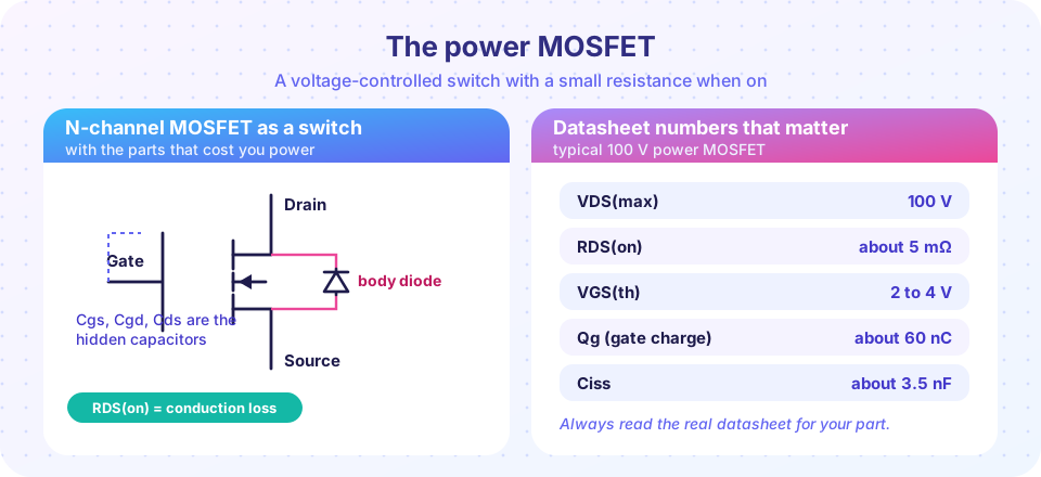
A power MOSFET is usually a vertical structure: current flows from the drain at the bottom of the chip up through the channel to the source on top. With VGS below the threshold VGS(th) (typically 2 V to 4 V), no channel exists and the device blocks voltage between drain and source. When VGS is raised well above threshold (10 V for standard devices, about 4.5 V for logic-level ones), the channel opens fully and the device behaves like a resistor RDS(on).
A MOSFET has three regions. In cutoff, it is off. In the ohmic (triode) region, it is on, acts like a resistor and is where a switch should live. In the saturation (active) region, the current is set by VGS, which is how analog amplifiers use it but a place where a switch dissipates a lot of power. During switching, the device crosses the active region quickly.
Conduction loss and temperature
Pcond = Irms² × RDS(on)
RDS(on) increases with temperature, roughly doubling between 25 °C and 125 °C for many silicon parts. Always use the hot value for loss and thermal design. Example: a 100 V MOSFET with RDS(on) = 5 mΩ at 25 °C and about 8 mΩ at 125 °C carrying 20 A rms dissipates 20² × 0.008 = 3.2 W when hot.
A useful property: this positive temperature coefficient lets MOSFETs be paralleled easily. If one device gets hotter, its resistance rises and it takes less current, so the current balances itself.
Voltage rating versus RDS(on)
Higher voltage rating means a thicker, lighter-doped drift region, and for conventional silicon RDS(on) per unit area grows roughly with the square or more of the breakdown voltage. A 30 V device may have 2 mΩ in a small package, while a 600 V device of the same size may have 100 mΩ or more. Super-junction structures reduce this penalty at 500 V to 900 V. This is the reason silicon MOSFETs are used below about 650 V to 900 V, while IGBTs and SiC take over at higher voltage.
Gate charge, the Miller plateau and gate-drive loss
The gate looks like a capacitor to the driver, but its value changes during switching. The datasheet gives gate charge Qg instead of a single capacitance. Turning on has three phases:
- Charging
Cgs:VGSrises to the threshold. The drain current starts to flow. - The Miller plateau:
VGSstays flat (typically 4 to 6 V) while the driver chargesCgdand the drain voltage falls. The charge in this phase isQgd. - Full enhancement:
VGSrises to the final drive voltage (for example 10 V), loweringRDS(on).
The time for each phase is charge / gate current. With Qg = 60 nC and a driver delivering 1 A, turn-on takes about 60 ns, and Qgd governs how fast the voltage can fall. The average gate-drive power is Pgate = Qg × Vgs × fsw, which for 60 nC, 10 V and 200 kHz is 0.12 W.
A fast gate drive lowers switching loss but makes dv/dt and di/dt larger, which increases noise. Designers choose a gate resistor to trade speed against electromagnetic interference.
The body diode
Every power MOSFET contains a parasitic diode from source to drain. It is useful: in a half-bridge, it carries the load current during dead time, and it can be used as the freewheeling diode. But a body diode of a high-voltage MOSFET is slow, with large Qrr, and can limit a design's efficiency or reliability. For hard-switched high-voltage half-bridges, designers choose devices with fast body diodes or use SiC or GaN.
Datasheet checklist
VDS(max): choose with margin, 20% to 50% above bus voltage depending on spikes.RDS(on)at the hot junction temperature and at your gate voltage.IDcontinuous (but check against thermal limits, not just the label).Qg,QgdandCiss,Coss,Crssfor switching speed and loss.- Maximum
VGS(commonly ±20 V; exceeding it destroys the gate oxide). - Body diode
Qrrif the diode conducts and recovers in your circuit. - Safe operating area (SOA) for linear operation or hard switching.
Common misconceptions
- "A MOSFET draws no current at the gate, so the driver can be tiny." Only the steady current is almost zero. Charging the gate in tens of nanoseconds needs amps of peak current from the driver.
- "A MOSFET is on when VGS passes threshold." At threshold the current is only microamps to milliamps. For full conduction you need the specified drive voltage, often 10 V.
Try it
The first demo is an interactive conduction-loss calculator with temperature scaling. Use it to see why a hot MOSFET loses more and why paralleling devices lowers the loss. This is a calculator for the formula P = I² × R with a simple linear model of resistance versus temperature.
Press Run (or Ctrl + Enter) to see the result here.
Program input · what you'd type while the program runs
Type the answers before you press Run, one per line. Each time the program reads a line (with input()), it gets the next line from this box.
Check your understanding
Quick check · 5 questions
of 5 answered You scored / 5 · perfect!
-
1. A MOSFET with RDS(on) = 4 mΩ (hot) carries 25 A rms. What is the conduction loss?
P = I² R = 625 × 0.004 = 2.5 W. -
2. What happens to RDS(on) as the junction heats up?
Silicon MOSFET resistance has a positive temperature coefficient, which helps paralleling. -
3. What does the Miller plateau represent?
VGS stays nearly constant while the drain voltage swings, because gate current is charging Cgd. -
4. Qg = 40 nC, Vgs = 12 V, fsw = 500 kHz. What is the gate-drive power?
Pgate = Qg × Vgs × fsw = 40e-9 × 12 × 500e3 = 0.24 W. -
5. Why does a 600 V silicon MOSFET have a much higher RDS(on) than a 30 V one of the same size?
Blocking high voltage needs a thick low-doped drift layer, which adds resistance.
Summary
- A MOSFET is a voltage-controlled switch; fully on it is a resistor
RDS(on). Pcond = I² × RDS(on); use the hot resistance, which can be double the cold one.- Gate charge
Qgsets drive current and gate-drive power; the Miller plateau governs the voltage fall. - The body diode is handy but slow in high-voltage MOSFETs.
- Check VDS, RDS(on), Qg, VGS limits and SOA on the datasheet.
Track your progress
Create a free account to tick off lessons and pick up where you left off on any device.
of Power Electronics lessons completed