


















Lesson 18 of 45 · DC-DC Converters
The Boost Converter: Stepping Voltage Up
Understand the boost converter: how an inductor steps voltage up, the 1/(1-D) gain, inductor and capacitor design, why high duty cycles fail, and a runnable simulation.
A boost converter makes a higher voltage from a lower one. It lights an LED string from a single battery cell, raises a solar panel's voltage, keeps 5 V on a USB port while a phone battery sags, and forms the front end of power-factor correction in a mains supply. At first glance it looks impossible: how can a passive inductor and a switch make more voltage out of less? The answer is that the inductor stores energy from the source and then adds its own voltage to the source's when the switch opens, like stacking two batteries for a moment.
What you will learn
- How the boost works in its two switch states and why
Vout = Vin / (1 − D). - Why the inductor current is larger than the load current.
- How to design
LandCand find the CCM boundary. - Why real boost converters cannot reach very high gains.
Key terms
- Boost converter: a DC-DC converter with the inductor in series with the input and a switch to ground.
- Average inductor current:
IL = Iout / (1 − D)in CCM. - Parasitic resistance: the unwanted resistance of the inductor, switch and diode.
- Right-half-plane zero: a feature of the boost's control behavior that limits loop speed.
- Input current ripple: here small, because the inductor is in the input path.
The two states
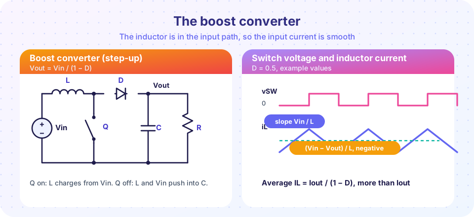
The inductor L is in series with the input source. The switch Q connects the node after the inductor to ground. The diode D carries current to the output capacitor C and load R.
- Q on (time
D T): the node is tied to ground, the inductor sees the fullVinand its current rises with slopeVin/L. The diode is off (the output is higher than the node), and the capacitor alone feeds the load, soVoutfalls slightly. - Q off (time
(1 − D) T): the inductor current cannot stop, so the node voltage rises until the diode conducts. The inductor now seesVin − Vout, which is negative ifVout > Vin, so its current falls. The inductor current flows through the diode, rechargingCand supplying the load.
Voltage gain. Volt-second balance: Vin × D T + (Vin − Vout)(1 − D) T = 0, so Vin = Vout (1 − D) and
Vout = Vin / (1 − D)
Currents. The diode carries the inductor current only during the off time, so the average diode current equals the load current, Iout = IL (1 − D). The average inductor (and input) current is
IL = Iout / (1 − D)
which is larger than the load current, since the input must supply Pin = Pout: Vin IL = Vout Iout. For a boost with D = 0.75, the input current is four times the output current.
Ripple. During the on time: ΔIL = Vin D / (L fsw). The output capacitor supplies the full load current while the switch is on, so
ΔVout ≈ Iout D / (fsw C)
Compare this with the buck: the boost's capacitor ripple has no 1/8 factor because its output current is pulsed (the diode conducts only part of the time), so it needs more capacitance for the same ripple.
Design example
Make Vout = 12 V from Vin = 5 V, Iout = 1 A at fsw = 200 kHz.
- Duty cycle:
D = 1 − Vin/Vout = 1 − 5/12 = 0.583. - Average inductor current:
IL = 1 / 0.417 = 2.4 A. - Choose ripple of 30% of
IL, soΔIL ≈ 0.72 A:L = Vin D / (fsw ΔIL) = 5 × 0.583 / (200 kHz × 0.72 A) = 20 µH. Pick22 µH:ΔIL = 0.66 A. - Peak inductor current:
2.4 + 0.33 = 2.73 A, so choose a saturation current of at least 3.5 A. The switch must carry that peak. - Output ripple target
50 mV:C = Iout D / (fsw ΔV) = 1 × 0.583 / (200 kHz × 0.05 V) = 58 µF. - The CCM boundary inductance is
Lcrit = D (1 − D)² R / (2 fsw)withR = 12 Ω: about3 µH. With22 µHthe converter stays in CCM down to light loads. - The switch must block
Vout(12 V plus spikes), so a 30 V MOSFET is a sensible choice.
Limits of the ideal formula
The ideal gain 1/(1 − D) rises without bound as D → 1, but a real converter has resistances in the inductor, the switch and the diode. Including the inductor's series resistance RL:
Vout / Vin = 1/(1 − D) × 1 / (1 + RL / (R (1 − D)²))
As D grows, the current grows too and the resistive drop grows with the square of 1/(1 − D), so the gain peaks and then falls. In practice, designers limit the duty cycle to about 0.8 to 0.85 and use a different topology (a transformer-based converter) for gains above 5 or 6.
Other things to know
- Input current is smooth. The inductor is in the input path, which makes the boost excellent as a PFC stage and for sources that dislike pulsed current, such as solar panels.
- No built-in short-circuit protection. If the output is shorted, the diode path connects the input directly to the short, so a fuse or active protection is needed. Also at start-up, the output capacitor charges through the inductor and diode, causing inrush current unless the design includes a soft start or a bypass.
- Right-half-plane zero. When the load increases, the controller raises
D, which first reduces the diode conduction time and makes the output voltage dip before it rises. This non-minimum-phase behavior limits the speed of the control loop. We will meet it in chapter 6.
Common misconceptions
- "A boost makes power from nothing." Input and output powers are equal (minus losses). Higher output voltage means lower output current, and the input current is higher than the output current.
- "The boost has the diode at the switch node for no reason." The diode is what prevents the output capacitor from discharging into the switch when it is on. Without it, the converter would short the output.
Try it
The simulation below integrates the boost converter equations with an ideal switch and diode. You can watch the start-up and the steady-state ripple, and compare the simulated average inductor current and ripple with the formulas. This model has no resistance, so it follows the ideal 1/(1 − D) gain.
Press Run (or Ctrl + Enter) to see the result here.
Program input · what you'd type while the program runs
Type the answers before you press Run, one per line. Each time the program reads a line (with input()), it gets the next line from this box.
Second, the effect of parasitic resistance. The plot shows the gain of a boost with an inductor resistance of 0.2 Ω feeding a 12 Ω load, using the formula in the lesson (an analytical model, not a simulation).
Press Run (or Ctrl + Enter) to see the result here.
Program input · what you'd type while the program runs
Type the answers before you press Run, one per line. Each time the program reads a line (with input()), it gets the next line from this box.
Check your understanding
Quick check · 5 questions
of 5 answered You scored / 5 · perfect!
-
1. A boost converter runs from 6 V at D = 0.5. What is Vout (ideal)?
Vout = Vin / (1 − D) = 6 / 0.5 = 12 V. -
2. A boost delivers 24 V at 1 A from a 12 V source (ideal). What is the average input current?
Pin = Pout = 24 W, so Iin = 24 / 12 = 2 A. That equals Iout/(1 − D) with D = 0.5. -
3. Why is the capacitor of a boost larger than a buck's for the same ripple?
In the buck, the inductor current smooths the output. In the boost, the diode current is pulsed. -
4. What limits the useful gain of a real boost converter at duty cycles above about 0.8?
Inductor and switch resistance cause drops that grow as 1/(1−D)², so the gain peaks and then falls. -
5. What is special about the input current of a boost?
The inductor in the input path keeps the input current continuous.
Summary
- Boost gain is
1/(1 − D); it steps up only. - Average inductor current
IL = Iout/(1 − D); rippleΔIL = Vin D/(L fsw); output rippleIout D/(fsw C). - The input current is smooth; the output current is pulsed, so the capacitor is large.
- Parasitic resistance caps the gain; avoid duty cycles above about 0.8 to 0.85.
- Protect against output shorts and start-up inrush, and remember the right-half-plane zero.
Next: The Buck-Boost Converter
Track your progress
Create a free account to tick off lessons and pick up where you left off on any device.
of Power Electronics lessons completed