


















Lesson 38 of 45 · Solid State and Bioinorganic Chemistry
Band Theory: Metals, Semiconductors and Insulators
See how molecular orbitals grow into bands, why a band gap separates conductors from insulators, and how doping and LEDs turn silicon into technology.
Every phone, solar panel and LED relies on one idea: how electrons fill the energy levels of a solid. Copper carries current with ease, diamond does not, and silicon sits in between and can be tuned. The difference is not in the atoms alone but in how their orbitals merge into bands. In this lesson you will build bands from the molecular orbital picture you already know and use them to explain conductivity, doping and the color of light-emitting diodes.
What you will learn
- Explain how N atomic orbitals combine into a band of N levels.
- Classify solids by band structure: metal, semiconductor, insulator.
- Describe intrinsic and extrinsic (n-type, p-type) semiconductors.
- Calculate the emission wavelength of an LED from its band gap.
- Explain why conductivity falls with temperature in metals and rises in semiconductors.
Key terms
Band: a quasi-continuous range of closely spaced energy levels formed from many atomic orbitals.
Valence band / conduction band: the highest filled band and the lowest empty band at absolute zero.
Band gap (Eg): the energy separation between the top of the valence band and the bottom of the conduction band.
Fermi level: the energy below which states are filled at 0 K.
Doping: adding a small amount of another element to supply extra electrons (n-type) or holes (p-type).
From orbitals to bands
Two atoms bring two atomic orbitals, giving two molecular orbitals (bonding and antibonding). Bring N atoms together and you get N molecular orbitals, spread over an energy range whose width depends on how strongly neighboring atoms overlap. With 10²³ atoms the levels are so close that they form an effectively continuous band. A sodium atom has one 3s electron; N sodium atoms have N electrons filling N/2 of the N levels of the 3s band. The band is half full, electrons just below the Fermi level can move to empty levels right above with almost no energy, and sodium is a metal.
Magnesium has a filled 3s band (two electrons per atom), yet is a metal because the 3s and empty 3p bands overlap, giving a continuous set of half-filled levels. Bands that do not overlap leave a gap.
Three kinds of solid
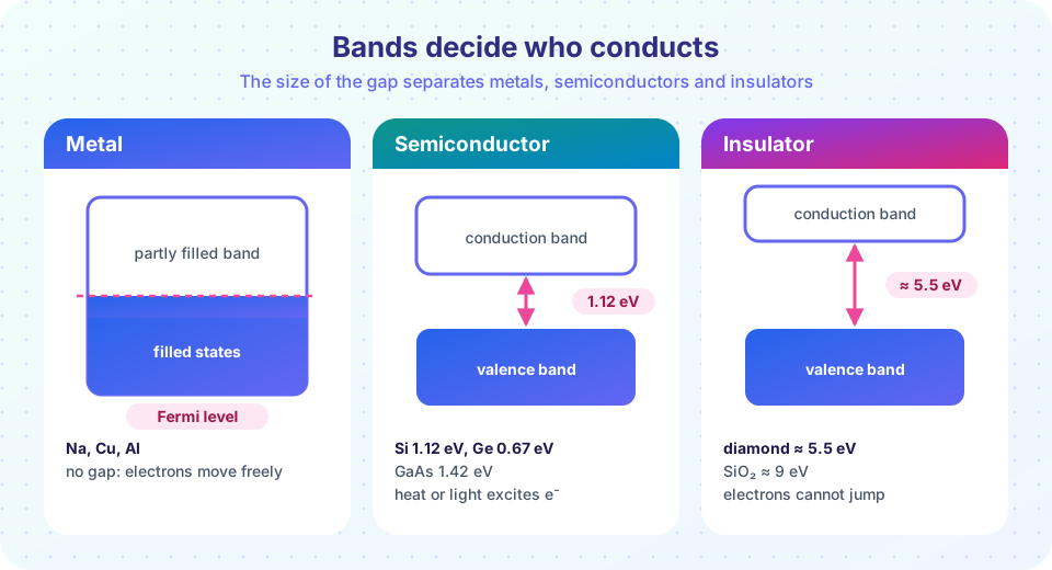
- Metals have a partly filled band (or overlapping bands), so electrons need almost no energy to move. Conductivity is high.
- Insulators have a full valence band, an empty conduction band, and a large gap (diamond about 5.5 eV, SiO₂ about 9 eV). At room temperature essentially no electrons can cross.
- Semiconductors have the same filled and empty bands but a small gap: Si 1.12 eV, Ge 0.67 eV, GaAs 1.42 eV. Thermal energy or light can lift a few electrons across, leaving holes in the valence band. Both electrons and holes carry current.
The dividing line between semiconductor and insulator is a convention near 3 eV. Thermal energy at 300 K is only kT ≈ 0.0259 eV, so excitation across a 1 eV gap is rare but not negligible: intrinsic silicon has about 10¹⁰ carriers per cm³, compared with about 10²² in a metal.
Temperature dependence
In a metal, conductivity falls as temperature rises: more lattice vibrations scatter the electrons. In a semiconductor, conductivity rises: the number of electrons promoted across the gap grows roughly as exp(−Eg / 2kT), which beats the scattering. That is why a thermistor made from semiconductor oxides is useful as a temperature sensor, and why a laptop chip must be cooled.
Doping
Pure silicon has few carriers. Adding impurities changes that dramatically:
- n-type: replace some Si (four valence electrons) with P or As (five). The extra electron sits in a donor level just below the conduction band and is easily promoted. Majority carriers are electrons.
- p-type: replace some Si with B or Ga (three valence electrons). The missing electron creates an acceptor level just above the valence band, which accepts electrons and leaves mobile holes.
Only about one atom in 10⁷ to 10⁹ needs to be replaced. Joining p-type and n-type silicon forms a p–n junction, the basis of diodes, transistors, solar cells and LEDs. In a solar cell, a photon with energy greater than Eg creates an electron–hole pair that the junction's electric field separates into a current. In an LED, the reverse happens: an electron falls across the gap and emits a photon of energy about Eg.
Gap and color
The wavelength of emitted light is λ (nm) = 1239.8 / Eg (eV). GaAs (1.42 eV) emits near 873 nm in the infrared, which is why it is used in infrared LEDs and remote controls. GaP (2.26 eV) gives about 549 nm, green. Blue LEDs needed a wide-gap material: GaN (3.4 eV, about 365 nm) alloyed with InN tunes the gap down into the blue, an achievement recognized by the 2014 Nobel Prize in Physics. Silicon's gap (1.12 eV, about 1107 nm) is indirect, which makes it a poor emitter but a good photodetector and solar cell material.
Common misconceptions
"Insulators have no band gap." They have a large gap. A semiconductor is just an insulator with a small gap.
"Holes are positrons." A hole is the absence of an electron in the valence band; it acts as a mobile positive charge carrier but is not a particle.
"Doping changes the number of atoms by a lot." One impurity in millions of atoms is enough.
Try it
Plot how the carrier fraction exp(−Eg / 2kT) grows with temperature for silicon, germanium and diamond. The curve is a simple Boltzmann-type model, not a full semiconductor calculation, and shows why a larger gap kills conduction.
Press Run (or Ctrl + Enter) to see the result here.
Program input · what you'd type while the program runs
Type the answers before you press Run, one per line. Each time the program reads a line (with input()), it gets the next line from this box.
The second tool converts a band gap into the wavelength and color of an LED. It uses λ = hc/Eg, where hc = 1239.84 eV·nm.
Press Run (or Ctrl + Enter) to see the console output here.
No output.
Check your understanding
Quick check · 5 questions
of 5 answered You scored / 5 · perfect!
-
1. Why is sodium a metal?
N sodium atoms supply N electrons for N levels in the 3s band, so the band is half filled. -
2. How does conductivity change with temperature in a semiconductor?
More electrons are excited across the gap as temperature rises. -
3. Phosphorus-doped silicon is...
Phosphorus has five valence electrons, so it donates an extra electron. -
4. What is the emission wavelength of an LED with Eg = 2.48 eV?
λ = 1239.84 / 2.48 ≈ 500 nm. -
5. Which has the largest band gap?
Diamond is about 5.5 eV, far larger than the others.
Summary
- N atomic orbitals form a band of N levels; the band filling and gap decide whether a solid conducts.
- Metals have partly filled bands, semiconductors small gaps and insulators large gaps.
- Semiconductor conductivity increases with temperature; metal conductivity decreases.
- Doping (n-type with P, p-type with B) tunes semiconductors, and p–n junctions power diodes, solar cells and LEDs.
- LED wavelength is 1239.8 / Eg (eV) nm.
Next: Bioinorganic Chemistry
Track your progress
Create a free account to tick off lessons and pick up where you left off on any device.
of Inorganic Chemistry lessons completed