


















Lesson 27 of 46 · Semiconductors and Metals
Intrinsic carriers and the mass-action law
Compute electron and hole densities in a pure semiconductor: effective density of states, the Fermi level at midgap, ni for silicon and the mass-action law.
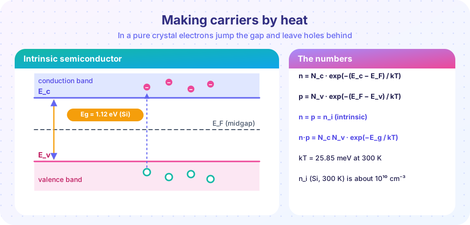
At absolute zero a pure semiconductor is an insulator: the valence band is full and the conduction band is empty. As you warm it, a few electrons gain enough thermal energy to jump the gap. Each jump creates two carriers: an electron in the conduction band and a hole in the valence band. How many? The answer is an exponential in Eg/2kT, and it sets the scale for almost everything in semiconductor physics.
What you will learn
- How to compute n and p from the effective density of states N_c, N_v and the Fermi level.
- Why the intrinsic Fermi level sits near midgap and how effective masses shift it.
- The mass-action law n p = n_i² = N_c N_v exp(−Eg/kT).
- How n_i changes with temperature and gap, and how to extract Eg from data.
Key terms
Effective density of states N_c, N_v: the number of states per unit volume that effectively sit at the band edge, N_c = 2(2π m_e* kT/h²)^(3/2).
Intrinsic carrier density n_i: the density of electrons (equal to the density of holes) in a pure crystal at temperature T.
Boltzmann approximation: valid when E_c − E_F and E_F − E_v exceed a few kT, so the Fermi-Dirac function becomes a simple exponential.
Mass-action law: n p = n_i², independent of doping in equilibrium.
Counting carriers
Near the bottom of the conduction band the energy is E = E_c + ħ²k²/(2m_e*), so the density of states per volume is g_c(E) = (1/2π²)(2m_e*/ħ²)^(3/2) sqrt(E − E_c). The electron density is the integral of g_c(E) f(E) dE with the Fermi-Dirac function f. If E_c − E_F ≫ kT, f ≈ exp(−(E − E_F)/kT) and the integral gives
n = N_c exp(−(E_c − E_F)/kT), with N_c = 2 (2π m_e* kT / h²)^(3/2)
Similarly for holes: p = N_v exp(−(E_F − E_v)/kT). For m* = m₀ and T = 300 K, N = 2.51 × 10¹⁹ cm⁻³. Silicon has N_c ≈ 2.8 × 10¹⁹ and N_v ≈ 1.0 × 10¹⁹ cm⁻³ at 300 K, using density-of-states effective masses m_e* ≈ 1.08 m₀ and m_h* ≈ 0.56 m₀.
In a pure crystal, n = p. Setting the two expressions equal gives the Fermi level
E_F = (E_c + E_v)/2 + (kT/2) ln(N_v/N_c) = (E_c + E_v)/2 + (3kT/4) ln(m_h*/m_e*)
which is within a few percent of midgap, because the logarithm is small compared with Eg/kT ≈ 43 for silicon. Multiplying the two expressions eliminates E_F and gives the mass-action law:
n p = N_c N_v exp(−Eg/kT) = n_i²
so n_i = sqrt(N_c N_v) exp(−Eg/2kT). Notice that n_i depends on the gap through exp(−Eg/2kT): half the gap, because each excitation creates a pair.
Numbers for silicon
At 300 K, kT = 0.02585 eV. For silicon with Eg = 1.12 eV: Eg/2kT = 21.7, exp(−21.7) = 3.9 × 10⁻¹⁰, and sqrt(N_c N_v) ≈ 1.7 × 10¹⁹ cm⁻³, giving n_i ≈ 7 × 10⁹ cm⁻³ in this simple model. Measured values are close to 10¹⁰ cm⁻³; the difference comes from temperature dependence of Eg and from approximate effective masses. Silicon has about 5 × 10²² atoms per cm³, so only about one in 10¹³ atoms contributes an electron-hole pair. In germanium (Eg = 0.66 eV) n_i ≈ 2 × 10¹³ cm⁻³, a couple of thousand times larger. In GaAs (Eg = 1.42 eV) n_i ≈ 2 × 10⁶ cm⁻³.
Temperature dependence is dominated by the exponential. Between 300 K and 400 K, silicon's n_i increases by a factor of a few hundred (it roughly doubles for every 10 K near room temperature), which is why intrinsic behavior limits devices at high temperature and why wide-gap semiconductors are preferred for hot environments.
Reading Eg from data
Taking logarithms, ln(n_i / T^(3/2)) = const − Eg/(2kT). Plotting against 1/T gives a straight line with slope −Eg/2k. This is how gaps are measured from conductivity or Hall data: an Arrhenius plot of the intrinsic range. Optical absorption gives the gap directly and provides a cross-check.
Common misconceptions
"Intrinsic means undoped, so n_i is zero at room temperature." It is small but finite; it grows exponentially with temperature and is the reference density for every doped sample.
"The Fermi level is a real energy level that electrons occupy." In the gap there are no states. E_F is a statistical quantity: the energy at which the occupation probability would be one half.
"n p = n_i² holds only for pure crystals." It holds for any nondegenerate semiconductor in thermal equilibrium, doped or not. Doping changes n and p in opposite directions with their product fixed.
Try it
Press Run (or Ctrl + Enter) to see the result here.
Program input · what you'd type while the program runs
Type the answers before you press Run, one per line. Each time the program reads a line (with input()), it gets the next line from this box.
Press Run (or Ctrl + Enter) to see the result here.
Program input · what you'd type while the program runs
Type the answers before you press Run, one per line. Each time the program reads a line (with input()), it gets the next line from this box.
Check your understanding
Quick check · 5 questions
of 5 answered You scored / 5 · perfect!
-
1. In an intrinsic semiconductor, the electron and hole densities satisfy
Each thermal excitation produces one electron and one hole. -
2. The mass-action law states that in equilibrium
n p = N_c N_v exp(−Eg/kT), independent of the doping level. -
3. Which change raises n_i the most?
n_i ∝ exp(−Eg/2kT), so halving Eg changes the exponent drastically. -
4. Where does the Fermi level lie in an intrinsic semiconductor?
Equal electron and hole densities put E_F at midgap, shifted slightly by the mass ratio. -
5. The slope of ln(n_i / T^(3/2)) against 1/T equals
n_i/T^(3/2) ∝ exp(−Eg/2kT), so the slope is −Eg/2k.
Summary
- n = N_c exp(−(E_c − E_F)/kT) and p = N_v exp(−(E_F − E_v)/kT) in the Boltzmann regime.
- In a pure crystal n = p = n_i = sqrt(N_c N_v) exp(−Eg/2kT), with E_F near midgap.
- The mass-action law n p = n_i² holds for doped crystals too.
- Silicon has n_i of about 10¹⁰ cm⁻³ at 300 K, germanium about 10¹³ and GaAs about 10⁶.
Track your progress
Create a free account to tick off lessons and pick up where you left off on any device.
of Condensed Matter Physics lessons completed