


















Lesson 26 of 46 · Semiconductors and Metals
Chapter 6 overview: semiconductors and metals
Preview chapter 6: how the band gap and the Fermi level determine whether a solid is a metal, semiconductor or insulator, and how doping and the Hall effect work.
Band theory gives a clean rule: a solid conducts when a band is partly filled. This chapter turns that rule into numbers. How many carriers does silicon have at room temperature? How does adding one phosphorus atom per million silicon atoms change its resistance by a factor of a thousand? How can a bar of semiconductor tell you whether the carriers are negative or positive? And why are all the diodes and transistors in your phone built on one crystal?
What you will learn
- How the size of the gap separates metals, semiconductors and insulators in practice.
- What "intrinsic", "doped", "electron" and "hole" mean.
- What the four lessons of this chapter deliver.
- Which quantities you will compute: carrier density, Fermi level, built-in voltage, Hall coefficient.
Key terms
Band gap Eg: the energy difference between the conduction band bottom (E_c) and the valence band top (E_v).
Hole: the absence of an electron in an almost full band, behaving as a positive charge carrier with positive effective mass.
Doping: adding impurity atoms (donors or acceptors) to control the carrier density.
Fermi level E_F: the chemical potential of the electrons; its position in the gap shows which carriers dominate.
The map of the chapter
Carriers from heat
Lesson 1: intrinsic carriers.
Carriers by design
Lesson 2: doping and junctions.
Measuring carriers
Lesson 3: Hall effect and mobility.
Metals, semiconductors, insulators in numbers
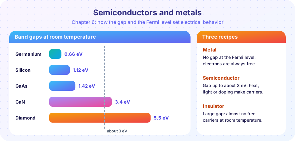
The dividing line is not sharp. A common working rule is that a solid with a gap below about 3 eV is called a semiconductor and above that an insulator, because 3 eV is roughly where thermal and optical excitation across the gap becomes negligible at room temperature. Metals have no gap at the Fermi level, so their conductivity is large (copper: about 6 × 10⁷ S/m) and falls slowly as they warm up because scattering increases. Semiconductors have a conductivity that is tiny at low temperature and rises exponentially as carriers are excited (pure silicon: about 3 × 10⁻⁴ S/m at room temperature, 11 orders of magnitude below copper). Insulators sit far below that.
The practical power of semiconductors comes from the fact that their carrier density can be set by the engineer, from about 10¹⁴ to 10²⁰ per cm³, by adding a trace of impurity, and then varied locally on a chip. Metals offer no such control, with carrier densities near 10²² to 10²³ per cm³ set by chemistry.
What each lesson covers
- Intrinsic carriers: electron and hole densities, the effective density of states and the mass-action law.
- Doping and the p-n junction: donors, acceptors, the Fermi level, the built-in voltage and the depletion layer.
- The Hall effect and mobility: how to measure the sign and the number of carriers.
- Chapter review: a recap table and ten questions.
Common misconceptions
"Insulators and semiconductors are different kinds of materials." They are the same in principle; only the gap size differs. Diamond is an insulator at room temperature, but its carriers can be made visible with doping, and wide-gap semiconductors such as GaN and SiC are the basis of power electronics.
"Metals conduct better at lower temperature because there are more electrons." The number of conduction electrons is almost fixed; what changes is the scattering time, which grows when phonons freeze out.
Try it
Press Run (or Ctrl + Enter) to see the result here.
Program input · what you'd type while the program runs
Type the answers before you press Run, one per line. Each time the program reads a line (with input()), it gets the next line from this box.
Press Run (or Ctrl + Enter) to see the result here.
Program input · what you'd type while the program runs
Type the answers before you press Run, one per line. Each time the program reads a line (with input()), it gets the next line from this box.
Check your understanding
Quick check · 4 questions
of 4 answered You scored / 4 · perfect!
-
1. Why is the dividing line between semiconductors and insulators placed near 3 eV?
The line is a convention: carrier excitation falls off exponentially with Eg/kT. -
2. A hole is best described as
The collective motion of the electrons around an empty state acts as a positive charge carrier. -
3. What gives a semiconductor engineer control over carrier density?
Even parts-per-million impurities change the carrier density by orders of magnitude. -
4. The conductivity of a metal usually
More phonon scattering shortens the electron lifetime.
Summary
- The gap size sorts solids: zero for metals, below about 3 eV for semiconductors, larger for insulators.
- Holes are the carriers of an almost full band.
- Doping lets engineers set the carrier density over many orders of magnitude.
- The chapter covers intrinsic carriers, doping and p-n junctions, and the Hall effect.
Next: Intrinsic carriers
Track your progress
Create a free account to tick off lessons and pick up where you left off on any device.
of Condensed Matter Physics lessons completed