


















Lesson 28 of 46 · Semiconductors and Metals
Doping and the p-n junction
Learn how donors and acceptors set carrier density, where the Fermi level sits, how a p-n junction forms a built-in voltage and a depletion layer, and the ideal diode law.
Pure silicon is a poor conductor. Add one phosphorus atom for every ten million silicon atoms and its conductivity jumps by a factor of about a million. This is doping, and it is the foundation of every diode, transistor and solar cell. Join a region doped with one type of impurity to a region doped with the other and you get a p-n junction: a device that conducts in one direction and blocks in the other, with a built-in electric field and an energy barrier you can calculate from first principles.
What you will learn
- How donors and acceptors add electrons or holes, and how big the binding energy is.
- How to find n, p and the Fermi level for a given doping.
- How the built-in voltage, depletion width and ideal diode law follow.
- What forward and reverse bias do to the barrier.
Key terms
Donor: an impurity with one extra valence electron (P, As or Sb in Si) that ionizes into the conduction band, leaving a fixed positive charge.
Acceptor: an impurity with one fewer valence electron (B, Al, Ga in Si) that takes an electron from the valence band, creating a hole and a fixed negative charge.
Depletion region: the layer at a junction emptied of mobile carriers, containing only fixed ionized impurities.
Built-in voltage V_bi: the electrostatic potential difference between the neutral n and p regions at equilibrium.
Donors and acceptors
A phosphorus atom replaces silicon and has five valence electrons. Four make bonds; the fifth is bound to the extra +1 charge of the phosphorus ion, like an electron in a hydrogen atom, but the crystal changes the numbers. The attraction is reduced by the dielectric constant ε_r ≈ 11.7 and the electron has effective mass m* ≈ 0.26 m₀ (conductivity mass), so the binding energy is about 13.6 eV × (m*/m₀)/ε_r² ≈ 26 meV and the orbit radius is 0.53 Å × ε_r m₀/m* ≈ 2.4 nm, many lattice spacings. The measured value for P in Si is 45 meV (the simple model is only an estimate). Since kT = 26 meV at room temperature, nearly all donors are ionized: at 300 K the electron density is set by the donors, n ≈ N_D. Acceptors work the same way with holes (boron in Si: 45 meV).
With both types present they compensate each other. In general, with all impurities ionized, charge neutrality p + N_D − n − N_A = 0 together with n p = n_i² gives
n = ½ [(N_D − N_A) + sqrt((N_D − N_A)² + 4 n_i²)]
For N_D − N_A ≫ n_i this is simply n ≈ N_D − N_A and p = n_i²/n.
Example. Silicon with N_D = 10¹⁶ cm⁻³ and n_i = 10¹⁰ cm⁻³: n = 10¹⁶, p = 10²⁰/10¹⁶ = 10⁴ cm⁻³. The electron-to-hole ratio is 10¹²: the minority carriers are almost absent. The Fermi level is E_F − E_i = kT ln(n/n_i) = 0.02585 × ln(10⁶) = 0.357 eV above the intrinsic level, close to the conduction band (the gap is 1.12 eV so E_i is near 0.56 eV above E_v). The conductivity is σ = e n μ_n ≈ 1.6 × 10⁻¹⁹ C × 10¹⁶ cm⁻³ × 1350 cm²/(V·s) ≈ 2.2 S/cm (216 S/m), versus about 3 × 10⁻⁶ S/cm for pure silicon.
The p-n junction
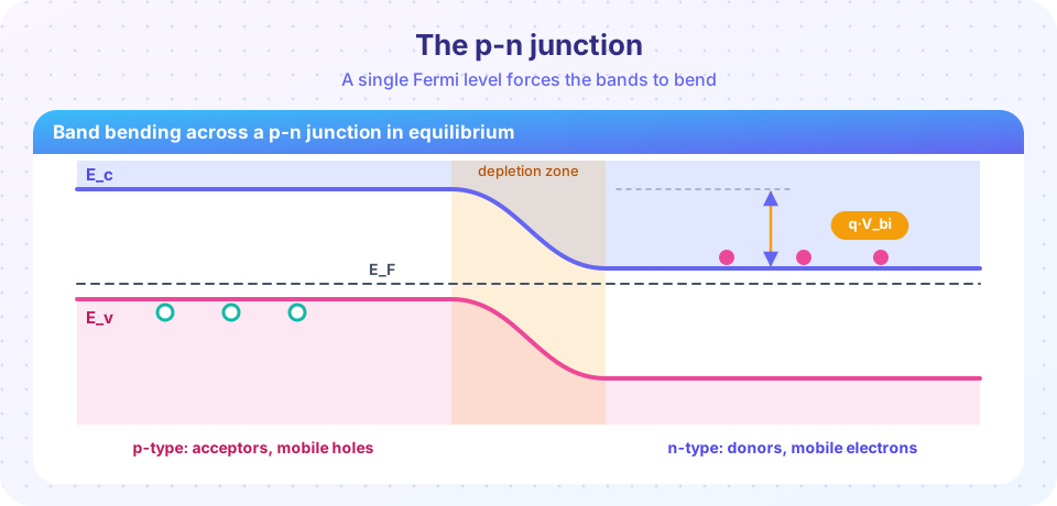
Place p-type (holes) and n-type (electrons) silicon in contact. Electrons diffuse from n to p and holes from p to n. Each carrier leaves behind a fixed ionized impurity, so a region around the interface becomes charged: positive on the n side (ionized donors), negative on the p side (ionized acceptors). This space charge creates an electric field that opposes further diffusion. At equilibrium diffusion and drift balance and the Fermi level is the same on both sides, which forces the bands to bend by
q V_bi = kT ln( N_A N_D / n_i² )
Example: N_A = 10¹⁷, N_D = 10¹⁶: V_bi = 0.02585 × ln(10³³/10²⁰) = 0.02585 × 29.9 ≈ 0.77 V. The width of the depletion layer, from Poisson's equation with the abrupt-junction approximation, is
W = sqrt( 2 ε (V_bi − V) / q × (1/N_A + 1/N_D) )
with ε = 11.7 ε₀ = 1.04 × 10⁻¹² F/cm for silicon. For the same doping this gives W ≈ 0.33 µm at zero bias. The depletion layer extends mostly into the lightly doped side: x_n = W N_A/(N_A + N_D), x_p = W N_D/(N_A + N_D).
Biasing the junction
Apply a voltage V (positive on the p side). Forward bias (V > 0) lowers the barrier to q(V_bi − V), more carriers diffuse across, and the depletion layer shrinks. Reverse bias (V < 0) raises the barrier and widens the layer. The ideal diode (Shockley) equation for the current is
I = I_s [ exp(qV / kT) − 1 ]
At room temperature kT/q = 25.85 mV, so each 60 mV of forward voltage raises the current by a factor of ten (at the ideal slope). Real silicon diodes switch on near 0.6 to 0.7 V because the saturation current I_s is very small (typical 10⁻¹² to 10⁻¹⁵ A), and they show recombination currents with an ideality factor between 1 and 2.
Common misconceptions
"n-type material has a net negative charge." It is electrically neutral: the extra electrons are balanced by positive donor ions fixed in the lattice.
"The built-in voltage can drive a current through an external wire." At equilibrium there is no net current; the contact potentials at the metal electrodes cancel V_bi exactly. A voltmeter across an isolated diode reads zero.
"The depletion layer contains no charge." It contains no mobile charge; the fixed ionized impurities are exactly what produce the field.
Try it
Press Run (or Ctrl + Enter) to see the result here.
Program input · what you'd type while the program runs
Type the answers before you press Run, one per line. Each time the program reads a line (with input()), it gets the next line from this box.
Press Run (or Ctrl + Enter) to see the result here.
Program input · what you'd type while the program runs
Type the answers before you press Run, one per line. Each time the program reads a line (with input()), it gets the next line from this box.
Check your understanding
Quick check · 6 questions
of 6 answered You scored / 6 · perfect!
-
1. In n-type silicon with N_D = 10¹⁶ cm⁻³ and n_i = 10¹⁰ cm⁻³, the hole density is about
p = n_i²/n = 10²⁰/10¹⁶ = 10⁴ cm⁻³. -
2. Why is a donor ionized at room temperature?
A hydrogen-like orbit scaled by ε_r and m* binds the electron only weakly. -
3. The built-in voltage of a silicon junction depends on doping through
Flat Fermi level across the junction gives q V_bi = kT ln(N_A N_D / n_i²). -
4. Reverse bias on a p-n junction
The external voltage adds to V_bi, increasing the voltage across the layer, so W grows as sqrt(V_bi − V). -
5. The forward current of an ideal diode rises by a factor of 10 for roughly each
ln(10) × kT/q ≈ 59.5 mV at 300 K. -
6. In a junction with N_A ≫ N_D the depletion layer extends mainly into
Charge neutrality N_A x_p = N_D x_n puts the longer layer on the lightly doped side.
Summary
- Donors and acceptors, ionized at room temperature, set n ≈ N_D − N_A and p = n_i²/n.
- The Fermi level moves toward the band that supplies the majority carriers: E_F − E_i = kT ln(n/n_i).
- A p-n junction has a built-in voltage q V_bi = kT ln(N_A N_D/n_i²) and a depletion width W ∝ sqrt(V_bi − V).
- The ideal diode current is I = I_s[exp(qV/kT) − 1].
Track your progress
Create a free account to tick off lessons and pick up where you left off on any device.
of Condensed Matter Physics lessons completed