


















Lesson 13 of 46 · Smith Chart and Matching
Lumped-Element Matching: Designing L-Networks
Design an L-match from two parts: pick the topology, compute Q, the series reactance and the shunt susceptance, choose low-pass or high-pass, and check the bandwidth.
Matching means making the impedance seen by a source equal to what the source wants, usually Z0, so that no power is reflected and the maximum is delivered. The simplest matching network is an L-network: one series element and one shunt element, shaped like the letter L. With only two parts you can match any two resistances, and the equations are short enough to solve on a napkin.
This lesson shows how the L-match works, how to design one for a real load and what bandwidth to expect.
What you will learn
- How an L-network transforms a resistance by creating a temporary series equivalent of a parallel circuit.
- The design equations for
Q, the series reactance and the shunt susceptance. - How to choose between the low-pass and high-pass versions.
- How to read bandwidth from the loaded Q, and how to handle a load that has reactance.
Key terms
- L-network: a two-element matching network with a series and a shunt element.
- Loaded Q:
Q = √(Rhigh/Rlow − 1), a measure of the impedance step and an indicator of bandwidth. - Susceptance (B): the imaginary part of admittance,
B = ωCfor a capacitor or−1/(ωL)for an inductor. - Low-pass match: series inductor and shunt capacitor; passes DC and attenuates harmonics.
- High-pass match: series capacitor and shunt inductor; blocks DC and attenuates low frequencies.
Why two parts are enough
A resistor R in parallel with a reactance Xp is equivalent, at one frequency, to a smaller resistor in series with a reactance:
Rs = R / (1 + Q²), Xs = Q Rs, with Q = R/|Xp|
A resistance is "transformed" down by the factor 1 + Q². Add a second element in series to cancel Xs and you have a pure resistance Rs instead of R. That is the L-match: the shunt element changes the load resistance, and the series element removes the leftover reactance. Taking the same idea backwards transforms resistances up.
The design equations
Let the lower resistance be Rlow and the higher be Rhigh. Always put the shunt element on the high-resistance side.
Q = √(Rhigh / Rlow − 1)
Xs = Q · Rlow (series reactance, on the low-resistance side)
Xp = Rhigh / Q (shunt reactance, across the high-resistance side)
The elements must have opposite signs. Choose between:
- Low-pass: series inductor
L = Xs / ω, shunt capacitorC = 1 / (ω Xp). - High-pass: series capacitor
C = 1 / (ω Xs), shunt inductorL = Xp / ω.
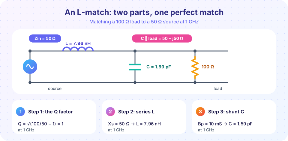
Worked example 1: 100 Ω load, 50 Ω source, 1 GHz, low-pass
Q = √(100/50 − 1) = 1.Xs = 1 × 50 = 50 Ω, soL = 50 / (2π × 10⁹) = 7.96 nH.Xp = 100 / 1 = 100 Ω, soC = 1 / (2π × 10⁹ × 100) = 1.59 pF.
Check: the load in parallel with the capacitor has admittance 0.01 + j0.01 S, which is 50 − j50 Ω. The inductor adds +j50 Ω, leaving exactly 50 Ω.
Worked example 2: the high-pass version
Xs = 50 Ω as a series capacitor: C = 1/(ω × 50) = 3.18 pF. Xp = 100 Ω as a shunt inductor: L = 100/ω = 15.9 nH. Check: 100 Ω ∥ j100 Ω has admittance 0.01 − j0.01 S, which is 50 + j50 Ω; the series capacitor adds −j50 Ω, giving 50 Ω.
Worked example 3: a load lower than the source
For RL = 20 Ω into 50 Ω, Rhigh = 50, Rlow = 20, so Q = √(50/20 − 1) = 1.225. The series element (Xs = 1.225 × 20 = 24.5 Ω) now sits next to the load and the shunt element (Xp = 50/1.225 = 40.8 Ω) goes across the source side. In every case the shunt part is on the side with the larger resistance.
Which version should I pick?
- Low-pass: the shunt capacitor gives a path to ground for harmonics, a useful bonus for power amplifiers. It also passes DC, so it cannot isolate bias.
- High-pass: series capacitors block DC and low-frequency noise; the shunt inductor gives a DC ground (useful as an ESD path).
- Parasitics decide at microwave frequencies. A 0.5 nH package inductance may be better absorbed into the series inductor of a low-pass design.
Bandwidth
The loaded Q of the L-match sets the sharpness of the match: a high impedance step (large Q) gives a narrow match. Since Q = √(Rhigh/Rlow − 1), a 2:1 step has Q = 1 while a 10:1 step has Q = 3. In the simulation below, the 100 Ω to 50 Ω low-pass match (Q = 1) keeps |Γ| ≤ 0.1 (return loss of at least 20 dB) from 846 to 1133 MHz, about 29% of the center frequency, while the 500 Ω to 50 Ω match (Q = 3) manages only 965 to 1034 MHz, about 7%. To widen the band, cascade two L-networks through an intermediate resistance: 50 → 22 → 10 has two sections of Q = 1.1 rather than one section of Q = 2.
Loads with reactance
If the load is RL + jXL, absorb its reactance into the matching element: a load inductor in series with the load can be treated as part of the series element, and a parallel capacitance as part of the shunt element. Design for the resistive part, then subtract the existing reactance from the calculated element.
Real components
- Inductors have finite Q (typically 30 to 100 for chip parts around 1 GHz). The resistive loss costs about
Q_loaded / Q_inductorof the power, so a high-Q match with a low-Q coil is lossy. - Capacitors have tolerance and self-resonance. Use
C0G/NP0types for RF and stay well below self-resonance. - Verify by measurement. Calculated values are a starting point and PCB layout adds a few tenths of a nanohenry.
Common misconceptions
- "A matching network amplifies power." It does not create power. It prevents reflection so more of the available power reaches the load.
- "One L-match works from DC to daylight." Every match is a narrowband solution around its design frequency.
- "The shunt part always goes at the source." It goes across the higher resistance, which is at the source only when
Rs > RL.
Try it
First, an interactive L-match designer. Type the source and load resistances and the frequency; the tool prints both versions and checks them.
Second, verify the design and see its bandwidth. The program builds both versions for 100 Ω into 50 Ω at 1 GHz and sweeps the frequency. It also tries a higher-Q step (500 Ω) to show how the band narrows.
Press Run (or Ctrl + Enter) to see the result here.
Program input · what you'd type while the program runs
Type the answers before you press Run, one per line. Each time the program reads a line (with input()), it gets the next line from this box.
Check your understanding
Quick check · 6 questions
of 6 answered You scored / 6 · perfect!
-
1. What loaded Q does an L-match from 50 Ω to 200 Ω have?
Q = √(200/50 − 1) = √3 = 1.73. -
2. In an L-match between a 50 Ω source and a 200 Ω load, where does the shunt element go?
The shunt element goes across the higher resistance, here the load. -
3. A low-pass L-match consists of
Series inductor and shunt capacitor pass low frequencies and attenuate harmonics. -
4. What series reactance Xs does the 100 Ω to 50 Ω match need?
Q = 1, Xs = Q × Rlow = 50 Ω. -
5. What happens to the bandwidth when the impedance step gets bigger?
Larger Q means a narrower match. -
6. A 2 nH series inductor already exists in the load. How do you account for it?
Absorb the existing reactance into the matching element.
Summary
- An L-network uses one series and one shunt element; the shunt goes across the higher resistance.
Q = √(Rhigh/Rlow − 1),Xs = Q Rlow,Xp = Rhigh/Q.- Low-pass: series L + shunt C; high-pass: series C + shunt L.
- Bandwidth is about
1/Q; use two sections to widen a large step. - Real parts have finite Q and parasitics: simulate, build, measure.
Track your progress
Create a free account to tick off lessons and pick up where you left off on any device.
of RF Engineering and Antennas lessons completed