


















Lesson 39 of 46 · Power Supplies and Practical Design
Switching regulators and practical power design
Understand the buck converter: duty cycle, inductor ripple, output ripple and efficiency versus linear regulators, plus decoupling, layout and protection habits.
A linear regulator turns the excess voltage into heat. If you must drop 12 V to 5 V at 1 A, you waste 7 W to deliver 5 W, and the regulator needs a heat sink. A switching regulator takes a different approach: it connects the input to an inductor in rapid pulses, and the inductor and capacitor smooth the pulses into the desired DC voltage. Because an ideal switch dissipates no power (either no voltage across it, or no current through it), the efficiency can be 90% or better.
This lesson explains the most common topology, the buck (step-down) converter, gives you the design equations, and then widens the view to the practical habits that decide whether your circuit works on the bench: decoupling, grounding, layout and protection.
What you will learn
- Explain how a buck converter works and derive
Vout = D · Vin. - Compute the inductor ripple current and output ripple voltage.
- Compare the efficiency of switching and linear regulators.
- Apply decoupling, layout and protection practices.
Key terms
Duty cycle (D): the fraction of each switching period during which the switch is on.
Switching frequency (fsw): how many on-off cycles per second; typically 100 kHz to several MHz.
Continuous conduction mode (CCM): operation where the inductor current never falls to zero.
Freewheel (catch) diode: the diode that carries the inductor current while the switch is off.
Decoupling capacitor: a capacitor placed across the supply pins of a chip to supply fast current and absorb noise.
How a buck converter works
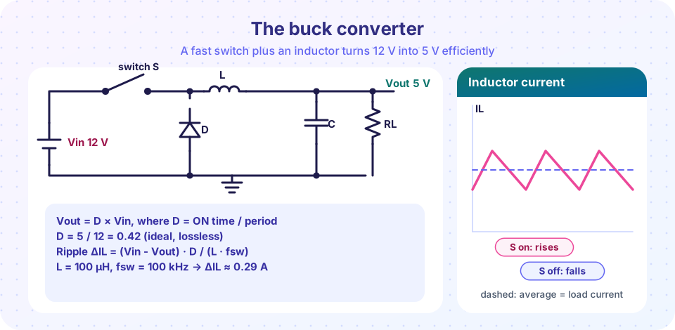
Refer to the picture. The switch S (a transistor in real life) alternately connects the left end of the inductor L to Vin and, through the diode, to ground.
- Switch on (time
D·T): the inductor seesVin - Voutacross it, so its current rises at(Vin - Vout) / L. It stores energy. - Switch off (time
(1 - D)·T): the inductor current cannot stop instantly; it keeps flowing through the diode and falls atVout / L. It releases energy to the load.
In steady state the inductor's current gains and loses the same amount per cycle, so the volt-seconds balance: (Vin - Vout) · D = Vout · (1 - D), which gives
Vout = D · Vin
The output is a lower voltage that you set by changing the duty cycle with a feedback controller. For 12 V in and 5 V out, D = 5/12 = 0.42.
Ripple current
The inductor current ramps up by
ΔIL = (Vin - Vout) · D / (L · fsw)
Worked example. Vin = 12 V, Vout = 5 V, L = 100 µH, fsw = 100 kHz, D = 0.417: ΔIL = 7 × 0.417 / (100×10⁻⁶ × 10⁵) = 0.29 A. If the load current is 1 A, the inductor current moves between about 0.85 A and 1.15 A. The usual design target is a ripple of 20-40% of the load current: too little and you need a huge inductor; too much and you increase losses and noise. A larger inductor or a higher frequency reduces ripple.
Output ripple voltage
The ripple current flows into the output capacitor C (the load takes the average). For an ideal capacitor,
ΔVout ≈ ΔIL / (8 · fsw · C)
With C = 100 µF: ΔVout = 0.29 / (8 × 10⁵ × 10⁻⁴) = 3.6 mV. In real capacitors the ESR (equivalent series resistance) dominates: ΔIL × ESR = 0.29 × 0.05 = 15 mV for a 50 mΩ capacitor. This is why low-ESR ceramic capacitors are favourites in switchers.
Efficiency
The losses of a real buck converter come from the switch's on-resistance (I² · Rds(on)), the diode drop (Vd · I, avoided with a synchronous MOSFET), the inductor winding resistance, the switching losses (voltage and current overlapping during edges) and the controller's own supply current. A typical well-designed converter reaches 85-95% at moderate load. Efficiency falls at very light loads, where fixed losses dominate; many controllers then enter a "pulse-skipping" or burst mode.
Other topologies
- Boost: steps voltage up,
Vout = Vin / (1 - D). - Buck-boost: can step up or down and inverts the polarity (in its basic form).
- Flyback: isolated, uses a coupled inductor: found in phone chargers.
The cost: noise
A switcher produces voltage and current edges that radiate and conduct noise at fsw and its harmonics. Analog circuits that need very low noise (sensors, audio, precision references) often take their power from a switcher followed by a small LDO, perhaps with an LC filter in between. The LDO's ripple rejection is good at low frequencies, but it falls off at the switching frequency, so the filter and layout matter.
Practical design habits
- Decouple every IC. Place a 100 nF ceramic capacitor between the supply pin and ground as close to the chip as possible, plus a larger bulk capacitor (1-10 µF, or more) near where power enters the board. The small capacitor supplies the fast current spikes that the long supply trace cannot.
- Keep the loops small. High-frequency current loops, such as the switch node in a converter, should be short and compact. Draw them on the board first.
- Think about return currents. Current flows in a loop: out on the supply and back on ground. A ground path that is long, thin or shared between analog and digital sections injects noise. Use a solid ground plane or a "star" ground for sensitive parts.
- Separate analog and digital where you can. Switching currents from digital circuits should not flow through the analog ground path.
- Protect the input. A fuse, a reverse-polarity diode (or P-channel MOSFET), and a TVS diode for surges prevent a cable mistake from destroying the board.
- Measure properly. Use a short oscilloscope ground spring, not a long ground lead, when looking at ripple; a long lead picks up and displays noise that is not really there.
Common misconceptions
"Switching regulators are always better." They add noise, cost and design complexity; at low power or low drop, an LDO is simpler and quieter.
"Decoupling capacitors can go anywhere." Distance adds inductance. A capacitor 5 cm away from the chip does little for megahertz noise.
"Higher switching frequency is free." It shrinks the inductor but raises switching losses and EMI.
Try it
The first example is a numerical simulation of the buck converter in the picture: a switch, a diode with a 0.5 V drop, a 100 µH inductor, a 100 µF capacitor and a 5 Ω load. It includes the diode drop but no other losses, so the real converter would be a little worse.
Press Run (or Ctrl + Enter) to see the result here.
Program input · what you'd type while the program runs
Type the answers before you press Run, one per line. Each time the program reads a line (with input()), it gets the next line from this box.
The second example compares the efficiency of a linear regulator and a buck converter as the load current changes. The buck loss model uses illustrative values for a 12 V to 5 V converter (on-resistance, diode drop, switching loss and a small controller current); it is a simple estimate, not a measurement.
Press Run (or Ctrl + Enter) to see the result here.
Program input · what you'd type while the program runs
Type the answers before you press Run, one per line. Each time the program reads a line (with input()), it gets the next line from this box.
The third example is a buck designer. Choose the voltages, frequency, inductor and load; it computes the duty cycle, ripple current and whether the converter stays in continuous conduction.
Check your understanding
Quick check · 5 questions
of 5 answered You scored / 5 · perfect!
-
1. An ideal buck converter has Vin = 24 V and D = 0.25. What is Vout?
Vout = D × Vin = 0.25 × 24 = 6 V. -
2. Which change reduces the inductor ripple current?
ΔIL = (Vin - Vout) D / (L fsw): larger L or fsw lowers the ripple. -
3. Why do linear regulators often follow switching regulators in low-noise designs?
The LDO filters residual ripple and noise, which sensitive analog stages cannot tolerate. -
4. Where should a 100 nF decoupling capacitor be placed?
Trace inductance makes a distant capacitor ineffective at high frequency. -
5. A buck converter feeds 5 V at 2 A from 12 V with 90% efficiency. What is the input power?
Output power is 10 W; input = 10 / 0.9 = 11.1 W, so 1.1 W is lost.
Summary
- A buck converter chops the input and averages it with an inductor and capacitor:
Vout = D · Vin. - Ripple current
ΔIL = (Vin - Vout) D / (L fsw); aim for 20-40% of the load current. - Switchers reach 85-95% efficiency but add noise; follow them with an LDO for sensitive analog circuits.
- Decouple every IC, keep high-frequency loops small, protect inputs, and measure with a short ground.
Next: Chapter review
Track your progress
Create a free account to tick off lessons and pick up where you left off on any device.
of Analog Electronics lessons completed