


















Lesson 19 of 46 · MOSFETs
The MOSFET small-signal model and the common-source amplifier
Linearize a MOSFET at its bias point, compute gm and ro, draw the small-signal model and find the gain, input and output resistance of a common-source amplifier.
The small-signal idea you met for the BJT carries over to the MOSFET with one convenient simplification: the gate takes no current, so the model has no base-style input resistor. The input is an open circuit, and the transistor is a voltage-controlled current source with a parallel output resistance. That is all.
This lesson derives the two parameters (g_m and r_o), builds a common-source amplifier, and compares it honestly with the BJT stage of chapter 3: lower gain for the same current, but a huge input resistance and a much larger linear range.
What you will learn
- How to derive g_m and r_o from the square-law current equation
- The three equivalent forms g_m = K·V_ov = 2I_D/V_ov = √(2K·I_D)
- How to find the gain and resistances of a common-source amplifier
- Why a MOSFET amplifier has less gain than a BJT but a far larger linear range
- How the intrinsic gain g_m·r_o limits a single stage
Key terms
Transconductance (g_m): ∂I_D/∂V_GS at the bias point; the small-signal current per volt at the gate.
Output resistance (r_o): 1/(λ·I_D); the slope of the output curve in saturation.
Common-source amplifier: input at the gate, output at the drain, source grounded for signals; the MOSFET counterpart of the common-emitter stage.
Intrinsic gain: the maximum voltage gain of a single transistor, g_m·r_o.
Source degeneration: a resistor in the source lead that trades gain for linearity.
Deriving g_m and r_o
In saturation, I_D = ½·K·(V_GS − V_th)²·(1 + λV_DS). Write v_GS = V_GS + v_gs and take the derivative with respect to the gate voltage:
gm = ∂ID/∂VGS = K · (VGS − Vth) = K · Vov
Because I_D = ½K·V_ov², we can rewrite this in three equivalent ways that are all useful:
gm = K · Vov = 2 · ID / Vov = √( 2 · K · ID )
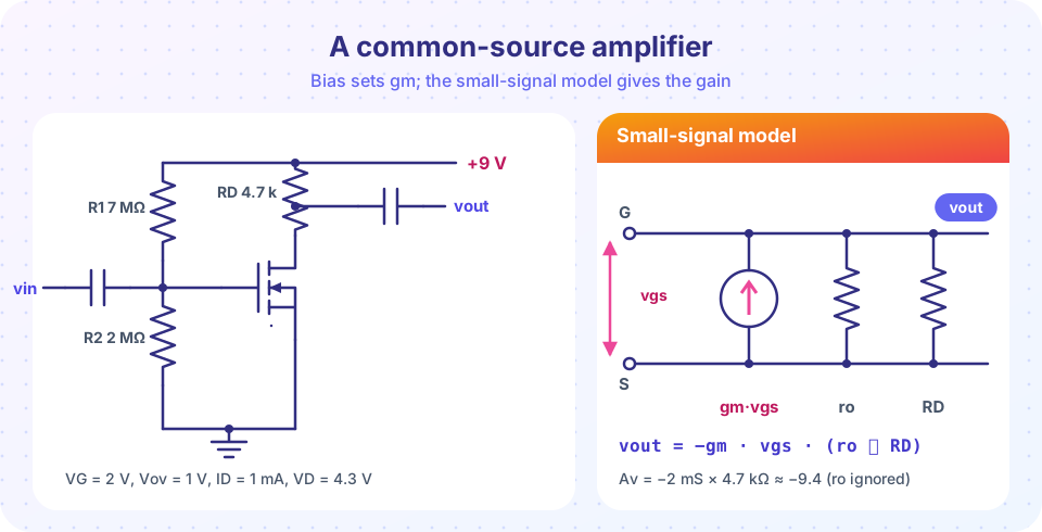
For our transistor (K = 2 mA/V², V_ov = 1 V, I_D = 1 mA): g_m = 2 mS. That is the same as 2 × 1 mA/1 V = 2 mS and √(2 × 0.002 × 0.001) = 2 mS.
The second parameter comes from the slight slope of the output curve in saturation:
ro = 1 / (λ · ID)
With λ = 0.02 V⁻¹ and I_D = 1 mA, r_o = 50 kΩ. The gate draws no DC current, so the gate-to-source resistance is infinite. The small-signal model is just two elements: a current source g_m·v_gs from drain to source, and r_o in parallel with it (right half of the figure).
The common-source amplifier
The circuit on the left of the figure applies the divider bias R₁ = 7 MΩ and R₂ = 2 MΩ to the gate. Because the gate draws no current, the divider is exact: V_G = 9 × 2/9 = 2 V. With the source at ground, V_GS = 2 V.
DC check. V_ov = 2 − 1 = 1 V, I_D = ½ × 2 mA × 1² = 1 mA. V_D = 9 − 1 mA × 4.7 kΩ = 4.3 V. V_DS = 4.3 V ≥ V_ov, so the transistor is in saturation. ✓ (This hand estimate ignores λ; including it raises I_D to about 1.09 mA, and the Python example below does that.)
Gain. For signals, the supply is ground and the output node sees R_D in parallel with r_o (and any load R_L). The output voltage is −g_m·v_gs times that combination, so
Av = −gm · ( RD ∥ ro ∥ RL )
- Ignoring r_o and the load: A_v = −2 mS × 4.7 kΩ = −9.4.
- Including r_o = 50 kΩ: 4.7 kΩ ∥ 50 kΩ = 4.30 kΩ, so A_v = −8.6.
- With a 10 kΩ load as well: 4.7 k ∥ 10 k ∥ 50 k = 3.0 kΩ, so A_v = −6.0.
Input and output resistance. R_in = R₁ ∥ R₂ = 1.56 MΩ, set entirely by the bias divider; the gate itself contributes nothing. R_out = R_D ∥ r_o ≈ 4.3 kΩ.
Comparing with the BJT stage
The BJT amplifier of the previous chapter, biased at 1.4 mA, had g_m = 54 mS and gain of about −254 with a similar collector resistor. At 1 mA the MOSFET has 2 mS: a factor of more than twenty lower, so the gain is lower by the same factor. The BJT wins for gain per milliamp. The MOSFET wins in three other ways:
- Input resistance. Megohms (limited by the bias network) rather than kilohms. It barely loads a high-impedance source.
- Linear range. The square-law current has only a small second-order term (see below).
- No base current, so the bias analysis is exact and simple.
Raising the gain
Since g_m = √(2K·I_D), you can raise the gain by increasing I_D (square-root dependence, slow), by increasing K through a larger W/L (quadrupling W/L doubles g_m at the same current), or by a larger R_D (limited by the supply voltage). The maximum for one transistor is the intrinsic gain:
gm · ro = (2·ID/Vov) · (1/(λ·ID)) = 2 / (λ · Vov)
For λ = 0.02 V⁻¹ and V_ov = 1 V this is 100. Lowering V_ov raises the intrinsic gain (but then the signal swing and speed suffer). Compare the BJT: g_m·r_o = V_A/V_T = 100 V / 25.9 mV = 3860. That is why single-stage BJT amplifiers can reach thousands where MOSFET stages reach tens to hundreds.
How linear is it?
Insert v_gs into the square law: I_D + i_d = ½K(V_ov + v_gs)² = ½K·V_ov² + K·V_ov·v_gs + ½K·v_gs². The middle term is the linear signal (g_m·v_gs). The last term is the second-order distortion, so
HD2 ≈ vgs / (4 · Vov)
For a BJT the corresponding figure was v_be/(4·V_T) with V_T = 25.9 mV. With V_ov = 1 V, the MOSFET tolerates a gate signal about 40 times larger for the same distortion: 100 mV peak gives about 2.5 %. A MOSFET stage can therefore handle bigger inputs, though with less gain per volt.
Source degeneration
A resistor R_S between source and ground (bypassed for DC stability or not) reduces the gain to
Av = −gm · RD / (1 + gm · RS)
For g_m·R_S ≫ 1 this tends to −R_D/R_S, fixed by resistor ratios, just like the BJT without a bypass capacitor. It also lowers distortion and shifts the bias point predictably.
Common misconceptions
"A MOSFET amplifier has more gain because the input resistance is infinite." Input resistance affects how much of the source signal arrives at the gate, not the transistor's own gain, which is g_m times the load resistance.
"g_m depends only on K." It depends on K and the bias current: g_m = √(2K·I_D).
"Small-signal theory ignores the DC bias." Bias sets g_m and r_o, and checking V_DS ≥ V_ov keeps the model valid.
Try it
First, a numerical check of the formulas. The program computes g_m by finite differences on the square law, compares it with the three closed forms, then analyzes the complete common-source stage including the load.
Press Run (or Ctrl + Enter) to see the result here.
Program input · what you'd type while the program runs
Type the answers before you press Run, one per line. Each time the program reads a line (with input()), it gets the next line from this box.
Second, a distortion experiment. A sine of increasing amplitude is applied to the square-law device. The Fourier transform of the output current measures the second harmonic; compare with the v_gs/(4·V_ov) rule, and with the BJT's far larger distortion for the same input.
Press Run (or Ctrl + Enter) to see the result here.
Program input · what you'd type while the program runs
Type the answers before you press Run, one per line. Each time the program reads a line (with input()), it gets the next line from this box.
Check your understanding
Quick check · 5 questions
of 5 answered You scored / 5 · perfect!
-
1. A MOSFET has K = 4 mA/V² and V_ov = 0.5 V. What is g_m?
g_m = K·V_ov = 4 mA/V² × 0.5 V = 2 mS. -
2. In saturation with I_D = 0.5 mA and V_ov = 0.25 V, g_m = 2I_D/V_ov equals:
g_m = 2 × 0.5 mA / 0.25 V = 4 mS. -
3. A common-source stage has g_m = 3 mS, R_D = 5 kΩ, no load, r_o very large. What is A_v?
A_v = −g_m·R_D = −0.003 × 5000 = −15. -
4. What sets the input resistance of the divider-biased common-source amplifier?
The gate is open for signals, so the input sees only the bias divider. -
5. Which has a larger intrinsic gain, a MOSFET (λ = 0.02, V_ov = 1 V) or a BJT (V_A = 100 V)?
BJT: V_A/V_T ≈ 3860. MOSFET: 2/(λ·V_ov) = 100.
Summary
- g_m = K·V_ov = 2I_D/V_ov = √(2K·I_D); r_o = 1/(λ·I_D).
- The MOSFET small-signal model: open gate, current source g_m·v_gs, r_o in parallel.
- Common-source gain: A_v = −g_m(R_D ∥ r_o ∥ R_L); R_in = R₁ ∥ R₂ (huge); R_out ≈ R_D ∥ r_o.
- Compared with a BJT, a MOSFET has much lower g_m and intrinsic gain, but far higher input resistance and a larger linear range (HD2 ≈ v_gs/(4V_ov)).
- Source degeneration reduces gain to about −R_D/R_S and improves linearity.
Next: Chapter 4 review
Track your progress
Create a free account to tick off lessons and pick up where you left off on any device.
of Analog Electronics lessons completed