


















Lesson 25 of 46 · Amplifier Basics and Biasing
Chapter 5 review: amplifier basics and biasing
Review gain, decibels, Q-point, divider bias and the common-emitter stage with a recap table, a design calculator, a frequency-response plot and a ten-question quiz.
You have now seen the whole life of a simple transistor amplifier: how to describe its gain, how to place its DC operating point, and how to predict what it does to a small AC signal. This review pulls the pieces into one picture and lets you test yourself with a design calculator and a quiz.
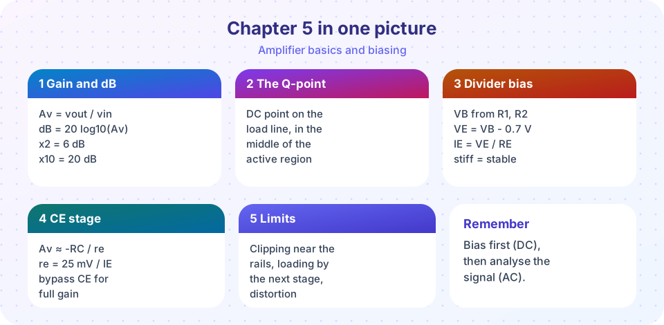
Recap table
| Idea | Key formula or rule | Where it came from |
|---|---|---|
| Voltage gain | Av = vout / vin |
Gain and decibels |
| Decibels | dB = 20 log10(Av); x2 = 6 dB, x10 = 20 dB |
same |
| Loading | Av0 · Rin/(Rs+Rin) · RL/(RL+Rout) |
same |
| Load line | VCE = VCC - IC (RC + RE) |
Biasing a bipolar transistor |
| Divider bias | VB = VCC R2/(R1+R2), VE = VB - 0.7, IE = VE/RE |
same |
| Target Q-point | VCE ≈ VCC / 2 |
same |
Small-signal re |
re = 25 mV / IE |
The common-emitter amplifier |
| CE gain | bypassed -RC / re; unbypassed -RC / (re + RE) |
same |
| Low-frequency corner | f = 1 / (2π R C) per capacitor |
same |
Putting it together: a design from scratch
Suppose you want an amplifier with VCC = 15 V, a collector current of 1 mA and the Q-point near the middle. A tidy way to reason:
- Choose
VE ≈ 1.5 V(a tenth of the supply), soRE = 1.5 kΩ. - Aim for
VCE = 7.5 V, soVC = 1.5 + 7.5 = 9 VandRC = (15 - 9) / 1 mA = 6 kΩ. VB = 1.5 + 0.7 = 2.2 V. With β = 150,IB = 6.7 µA; pick a divider current ten times larger, 67 µA, soR2 = 2.2 / 67 µA ≈ 33 kΩ.R1 = (15 - 2.2) / (67 µA + 6.7 µA) ≈ 174 kΩ.- Round to standard values and re-check the Q-point.
The calculator below does exactly that, rounds to the E12 preferred series and then re-analyses the real circuit, so you can see how much rounding matters. It models the DC circuit and the bypassed small-signal gain only.
Try it
Press Run (or Ctrl + Enter) to see the result here.
Program input · what you'd type while the program runs
Type the answers before you press Run, one per line. Each time the program reads a line (with input()), it gets the next line from this box.
The next plot shows how the three capacitors of a CE stage shape the low-frequency end of the response. It uses a simple model: each capacitor contributes a first-order high-pass corner. It is a simplified model, not a SPICE simulation.
Press Run (or Ctrl + Enter) to see the result here.
Program input · what you'd type while the program runs
Type the answers before you press Run, one per line. Each time the program reads a line (with input()), it gets the next line from this box.
Check your understanding
Quick check · 10 questions
of 10 answered You scored / 10 · perfect!
-
1. A stage with a voltage gain of 316 has what gain in decibels?
20 log10(316) = 20 × 2.5 = 50 dB. -
2. Which pair of statements about decibels is correct?
Voltage doubles at +6 dB. Power doubles at +3 dB (voltage rises by 1.41). -
3. An amplifier with open-circuit gain 50 has Rin = 10 kΩ, driven from Rs = 10 kΩ, and RL = Rout. What is the gain from source to load?
Input divider 0.5 and output divider 0.5: 50 × 0.5 × 0.5 = 12.5. -
4. In divider bias, which resistor turns the base voltage into the emitter current?
IE = (VB - 0.7) / RE, so RE sets the current. -
5. Why is the Q-point placed near VCC/2?
A centred Q-point gives symmetrical headroom in both directions. -
6. With IE = 2.5 mA and RC = 3 kΩ (emitter bypassed), what is the approximate unloaded gain?
re = 25 mV / 2.5 mA = 10 Ω, so Av = -3000 / 10 = -300. -
7. What happens to the DC bias if you add a bypass capacitor across RE?
The capacitor only affects AC. The DC Q-point stays the same. -
8. Which change reduces distortion of a CE stage at the cost of gain?
Unbypassed emitter resistance adds negative feedback and linearises the stage. -
9. A CE stage inverts the signal. What does that mean?
More input voltage raises collector current, lowering the collector voltage. -
10. The input coupling capacitor of 10 µF sees a total resistance of 2.5 kΩ. What is its corner frequency?
f = 1 / (2π × 2500 Ω × 10 µF) = 6.4 Hz.
Summary
- Gain multiplies as a ratio and adds in decibels; loading dividers reduce real gain.
- Bias with a divider and an emitter resistor; target
VCE ≈ VCC / 2. - A bypassed CE stage gives
Av = -RC / re; partial degeneration trades gain for linearity. - Each capacitor adds a low-frequency corner
1 / (2π R C).
Track your progress
Create a free account to tick off lessons and pick up where you left off on any device.
of Analog Electronics lessons completed