


















Lesson 16 of 46 · MOSFETs
Chapter 4 overview: the MOSFET
See the big picture of the MOSFET, the transistor behind almost every chip: how a gate voltage controls a channel, and how this chapter builds from the I-V curve to CMOS.
Open a smartphone and you will find tens of billions of MOSFETs, more than any other manufactured object in history. The metal-oxide-semiconductor field-effect transistor was first made to work at Bell Laboratories in 1959 by Mohamed Atalla and Dawon Kahng, building on the field-effect idea that Julius Lilienfeld had patented in the 1920s. It is the heart of microprocessors, memory, image sensors and most modern power switches, and it is a capable analog component too.
A MOSFET differs from a BJT in one important way. The BJT is controlled by a current (the base current) and so draws some input current all the time. The MOSFET is controlled by a voltage on an insulated gate. In steady state no current enters the gate at all, so the input resistance is enormous. That makes it ideal for high-impedance sensors, for digital logic that must not load its neighbors, and for switching large currents with almost no drive power.
What you will learn
- What a MOSFET is and how its terminals compare with a BJT's
- The central idea: a gate voltage creates a conducting channel
- The map of this chapter's lessons
- When to choose a MOSFET and when a BJT
Key terms
MOSFET: metal-oxide-semiconductor field-effect transistor; a voltage-controlled device with gate, drain, source (and body) terminals.
Gate, drain, source: the control terminal and the two ends of the conducting channel.
Threshold voltage (V_th): the gate-source voltage at which the channel forms.
NMOS and PMOS: n-channel and p-channel versions. This chapter's examples are mostly NMOS.
CMOS: complementary MOS, logic built from an NMOS and a PMOS transistor pair.
The central idea: a field makes a channel
Imagine a plate (the gate) separated from the silicon underneath by a very thin layer of insulating oxide. Applying a positive voltage to the gate attracts electrons to the surface of the p-type silicon below, forming a thin conducting layer, the channel, between two n-type regions called source and drain. Below the threshold voltage there is no channel and no current. Above it, the more positive the gate, the thicker and more conductive the channel, and the larger the drain current for a given drain voltage.
Because the gate is insulated, it behaves as a capacitor. Charging it takes a short pulse of current (so fast switching needs drive current), but once charged, no current flows. This is why a MOSFET's DC input current is essentially zero (picoamps from leakage).
Comparing BJT and MOSFET
| Property | BJT | MOSFET |
|---|---|---|
| Control | Base current | Gate voltage |
| DC input current | I_B = I_C/β | Essentially zero |
| I–V law | Exponential | Square law (saturation) |
| Transconductance at a given current | High (I_C/V_T) | Lower (2I_D/V_ov) |
| Typical on-state loss | V_CE(sat) of about 0.2 V | R_DS(on), as low as milliohms |
| Strongest at | Small-signal analog, high gain | Digital, power switching, high input impedance |
Both are useful. In analog design a BJT gives more gain per milliamp; a MOSFET gives a nearly infinite input resistance and, in modern processes, immense numbers of devices per chip. Many designs use both.
Chapter map
Device and curves
Switching
Amplifying
Same model idea as the BJT.
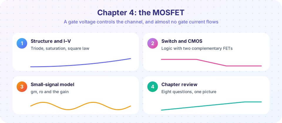
- Structure and I–V characteristics: cross-section, the three regions and the square law.
- The MOSFET as a switch and the CMOS inverter: R_DS(on), logic and power.
- The MOSFET small-signal model: g_m, r_o and the common-source amplifier.
- Chapter 4 review: one picture and ten questions.
Common misconceptions
"A MOSFET draws no current, so it needs no drive circuit." It draws none in steady state, but the gate capacitance must be charged and discharged each time it switches, which takes brief, sometimes large, current pulses.
"MOSFETs are always better than BJTs." For small-signal gain per milliamp, noise at low impedance and matching, BJTs often win. Pick the device for the job.
"The threshold voltage is the voltage at which the MOSFET switches fully on." It is the voltage at which the channel begins to form. Full conduction needs the gate several volts above it (for power devices, 4.5 V or 10 V).
Try it
First, a comparison of transconductance. At the same drain/collector current, how does a MOSFET compare with a BJT? The plot uses a MOSFET with K = 2 mA/V² (introduced in the next lesson) against an ideal BJT.
Press Run (or Ctrl + Enter) to see the result here.
Program input · what you'd type while the program runs
Type the answers before you press Run, one per line. Each time the program reads a line (with input()), it gets the next line from this box.
Second, a gate-voltage slider. As the gate voltage rises past the threshold, the channel thickens and the drain current rises. The model uses the square law with V_th = 1 V and K = 2 mA/V² at a fixed drain voltage of 5 V.
Check your understanding
Quick check · 4 questions
of 4 answered You scored / 4 · perfect!
-
1. What controls the drain current of a MOSFET?
A voltage on the insulated gate sets the channel and so the drain current. -
2. Why is a MOSFET's DC input current essentially zero?
The oxide layer insulates the gate, so no DC current flows into it. -
3. What is CMOS?
CMOS pairs complementary devices so that one is off whenever the other is on. -
4. At the same bias current, which device usually gives more transconductance?
The BJT's g_m = I_C/V_T is typically several times larger than a MOSFET's at the same current.
Summary
- A MOSFET's gate voltage forms a channel between source and drain; below V_th there is no channel.
- The gate is insulated, so DC gate current is essentially zero; switching still needs gate charge.
- MOSFETs excel at digital logic, power switching and high-impedance inputs; BJTs give more g_m per milliamp.
- The chapter covers structure and I–V, the switch and CMOS inverter, and the small-signal model.
Track your progress
Create a free account to tick off lessons and pick up where you left off on any device.
of Analog Electronics lessons completed