


















Lesson 41 of 46 · Projects and Practice
Project: a 20 dB audio preamplifier
Design an op-amp audio preamplifier from a specification: gain 11, 20 Hz to 20 kHz bandwidth, parts values, op-amp choice, offset and slew checks, and a test plan.
Theory becomes skill when you design something from a specification. In this project you will take a small, realistic requirement, a preamplifier for a weak audio source, and carry it from a blank page to a complete parts list with every check you learned in chapters 5 to 8. The method is the point: the same steps work for sensor amplifiers, instrumentation front ends and filters.
The specification. A source delivers up to 100 mV peak and has an output resistance of 1 kΩ. You need an output of at least 1 V peak (a gain of about 10), a passband of 20 Hz to 20 kHz, high input resistance so the source is not loaded, and operation from a symmetric ±9 V supply.
What you will learn
- Turn a specification into a topology and component values.
- Check bandwidth, slew rate, offset and bias-current error.
- Verify the response with a model before building.
- Plan the build and the tests.
Step 1: choose the topology
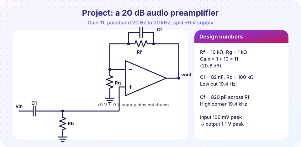
The requirement of "high input resistance" points straight to the non-inverting amplifier: its input is the + pin of the op-amp, which draws almost no current. The inverting amplifier would load the source with Rin. The gain of the non-inverting stage is 1 + Rf / Rg.
Step 2: gain resistors
Choose Rg = 1 kΩ. For a gain of 11, Rf = 10 kΩ (both standard values, 1% metal film for accuracy). The output for a 100 mV peak input is 1.1 V peak: a little above the 1 V requirement, which leaves margin for the loss from the source resistance (negligible here because the + input draws nanoamperes at most).
The resistors are low enough to keep thermal noise small and high enough not to load the op-amp: the feedback network draws only 1.1 V / 11 kΩ = 0.1 mA.
Step 3: the low-frequency cut
The input needs a DC path for the op-amp's bias current, so a resistor Rb goes from the + pin to ground, and a coupling capacitor C1 blocks DC from the source. They form a high-pass filter with fL = 1 / (2π Rb C1). For fL = 20 Hz with Rb = 100 kΩ, C1 = 1 / (2π × 100,000 × 20) = 79.6 nF, so use 82 nF (a film capacitor; avoid polarised parts here), giving fL = 19.4 Hz.
Rb also sets the input resistance of the amplifier at mid-band: 100 kΩ, which is 100 times the source's 1 kΩ, so the loss is 100 / 101, about 0.09 dB: negligible.
Step 4: the high-frequency roll-off
You may want to limit the bandwidth above 20 kHz to reduce noise and avoid picking up radio interference. A capacitor Cf in parallel with Rf makes the gain fall from 11 toward 1 above fH = 1 / (2π Rf Cf). For fH = 20 kHz: Cf = 1 / (2π × 10,000 × 20,000) = 796 pF, so use 820 pF (C0G ceramic), giving fH = 19.4 kHz. Note that this is a first-order roll-off that never goes below a gain of 1, a gentle high-cut rather than a brick wall.
Step 5: choose the op-amp and check the limits
Now return to the real-world limits from chapter 6.
- Bandwidth. The closed-loop gain is 11, and we want flat response to 20 kHz. Required GBW is at least
11 × 20 kHz = 220 kHz; with a safety factor of 10, aim for at least 2 MHz. A TL072-class part (GBW about 3 MHz) works. - Slew rate. The largest output is 1.1 V peak at 20 kHz:
2π × 20,000 × 1.1 = 0.14 V/µs. Even an old 0.5 V/µs part passes. - Offset. A bipolar op-amp with
Vos = 2 mVgives22 mVDC offset at the output (gain 11), tolerable because the output can be AC coupled. A bigger worry is the bias current: a bipolar input draws about 80 nA throughRb = 100 kΩ, creating 8 mV at the input, or 88 mV at the output. A JFET-input op-amp has bias currents of picoamperes, so this error disappears: another reason to prefer a TL072-class part here. - Output swing. ±9 V supply with a 1.1 V peak signal: plenty of room.
Step 6: power-supply details
Add 100 nF ceramic capacitors from each supply pin to ground, close to the chip, plus 10 µF electrolytics where the supply enters the board. If the supply comes from a switching converter, add a small LC or RC filter first. Keep the input wiring short and away from the output to prevent feedback and oscillation.
Step 7: verify before you build
The model below computes the exact response of the designed network, H(f) = H_highpass(f) × (1 + Zf / Rg) with Zf = Rf ∥ Cf, and confirms the corner frequencies and the gain at the points of interest.
Try it
The first example models the complete frequency response of the preamplifier from the component values. It assumes an ideal op-amp (the real GBW would only matter far above 100 kHz).
Press Run (or Ctrl + Enter) to see the result here.
Program input · what you'd type while the program runs
Type the answers before you press Run, one per line. Each time the program reads a line (with input()), it gets the next line from this box.
The second example runs the signal through the design: a 1 kHz tone at 100 mV peak plus 20 mV of 50 Hz hum. It prints the output peak, the slew requirement and the offset errors for two types of op-amp input. It models linear behaviour and the DC error budget only.
Press Run (or Ctrl + Enter) to see the result here.
Program input · what you'd type while the program runs
Type the answers before you press Run, one per line. Each time the program reads a line (with input()), it gets the next line from this box.
The third example is a tuner. Change the five component values and see the gain and both corner frequencies update.
Step 8: test plan
When you build the circuit, describe what you will measure and compare with the model (do not assume results in advance):
- Check the supply rails and the DC level at the output (should be small).
- Apply a 1 kHz sine at 100 mV peak and measure the output; compute the gain.
- Sweep the frequency from 10 Hz to 100 kHz at constant input amplitude and plot the gain; compare with the model.
- Increase the amplitude until the output clips; note the clipping level.
- Short the input and look for noise and hum at the output.
Check your understanding
Quick check · 5 questions
of 5 answered You scored / 5 · perfect!
-
1. Why is the non-inverting amplifier chosen for this preamplifier?
The requirement was a high input resistance; only the non-inverting stage provides it. -
2. With Rg = 2.2 kΩ and Rf = 22 kΩ, what is the gain?
1 + 22 / 2.2 = 11. -
3. Rb = 47 kΩ and C1 = 100 nF form which corner frequency?
f = 1 / (2π × 47,000 × 10⁻⁷) = 33.9 Hz. -
4. Why is a JFET-input op-amp preferred with a 100 kΩ bias resistor?
A bipolar input's 80 nA times 100 kΩ gives 8 mV at the input, amplified by the gain. -
5. What does the Cf capacitor across Rf do?
At high frequencies Cf shunts Rf, lowering the feedback impedance and the gain.
Summary
- Design from the requirement: topology, gain resistors, coupling and bias, bandwidth shaping, then check GBW, slew, offset and swing.
- Non-inverting gain
1 + Rf/Rg; low corner1/(2π Rb C1); high corner1/(2π Rf Cf). - Model the circuit before you build it, then compare your measurements with the model.
- Decoupling and layout belong to the design, not to an afterthought.
Track your progress
Create a free account to tick off lessons and pick up where you left off on any device.
of Analog Electronics lessons completed