


















Lesson 24 of 46 · Amplifier Basics and Biasing
The common-emitter amplifier
Analyse a common-emitter BJT stage with the small-signal model: gain -RC/re, input and output resistance, coupling and bypass capacitors, and distortion limits.
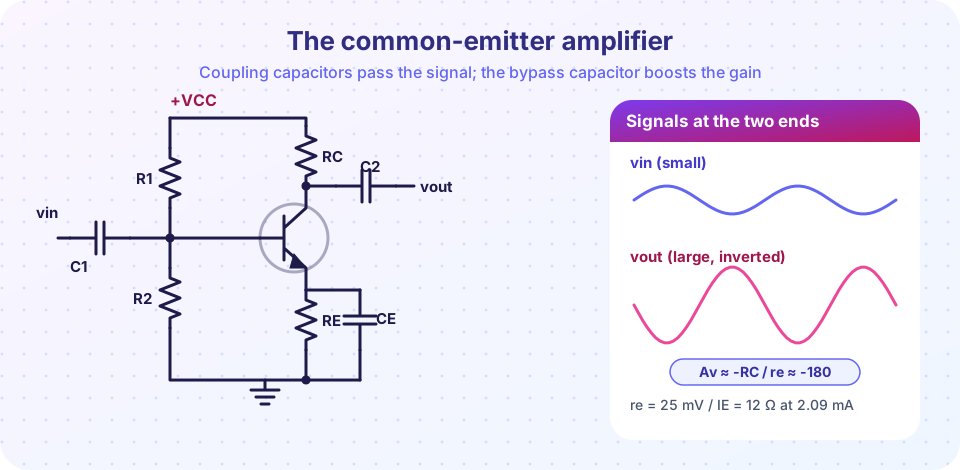
The common-emitter (CE) stage is the workhorse of discrete amplifier design. The input goes to the base, the output is taken from the collector, and the emitter is "common" to both in the AC sense (it is at, or close to, ground for the signal). It gives large voltage gain, moderate input resistance and a moderately high output resistance, which is why it appears in everything from audio preamps to radio front ends.
In the previous lesson you set the DC Q-point. Now you will switch to the AC view: replace the transistor by a tiny model that is valid for small signals, and use it to predict gain and resistances.
What you will learn
- Compute the emitter resistance
re = VT / IEand use it for the gain. - Predict the gain with and without an emitter bypass capacitor and with a load.
- Estimate input and output resistance of the stage.
- Explain what the coupling and bypass capacitors do and why the signal must stay small.
Key terms
Small-signal model: a linear approximation of a transistor valid only for signals small compared with the DC bias.
re: the transistor's small-signal emitter resistance, re = VT / IE with thermal voltage VT ≈ 25 mV at room temperature.
Coupling capacitor: a capacitor that passes the AC signal but blocks DC between stages.
Bypass capacitor: a capacitor across a resistor that gives the AC signal a short path around it.
Transconductance (gm): change in collector current per volt of base-emitter voltage, gm = IC / VT = 1 / re.
Why a transistor amplifies: the exponential law
The collector current of a BJT follows IC = IS · exp(VBE / VT), where IS is a tiny leakage constant of the device. Changing VBE by a small vbe changes the current by approximately ic = gm · vbe, where gm = IC / VT. At IC = 2 mA, gm = 2 mA / 25 mV = 80 mS. The collector current flows through RC, so the output voltage change is vout = -ic · RC = -gm · RC · vbe. The minus sign appears because more current drops more voltage across RC, pulling the collector down.
Gain of the stage
If the emitter is at AC ground (a bypass capacitor across RE), then vbe = vin and
Av = -gm · RC = -RC / re
Using the Q-point from the last lesson (IE ≈ 1.99 mA): re = 25 mV / 1.99 mA = 12.6 Ω, so the unloaded gain is Av = -2200 / 12.6 = -175, about 45 dB. If a load RL = 10 kΩ is connected through the output coupling capacitor, it appears in parallel with RC for the signal: RC ∥ RL = 1.8 kΩ, giving Av = -1800 / 12.6 = -143.
Without the bypass capacitor
Remove the bypass capacitor and RE is in the signal path, so the emitter moves too: only part of vin reaches the junction. The gain becomes
Av = -RC / (re + RE) = -2200 / (12.6 + 1000) = -2.2
That is a huge loss of gain, but there is a bonus: with RE unbypassed, the gain depends mostly on resistor ratios, not on re (which varies with temperature and the particular transistor). The circuit becomes much more linear and predictable. This is emitter degeneration, a form of negative feedback, and amplifier designers often split RE into a small unbypassed part and a larger bypassed part to choose gain on purpose.
Input and output resistance
The signal sees the base divider in parallel with the resistance looking into the base:
Rin = R1 ∥ R2 ∥ [β · (re + RE_unbypassed)]
With the bypass capacitor and β = 150: β · re = 150 × 12.6 = 1.89 kΩ, and R1 ∥ R2 = 7.67 kΩ, so Rin = 7.67 kΩ ∥ 1.89 kΩ = 1.52 kΩ. Not very high! If the source has Rs = 1 kΩ, the input divider keeps only 1.52 / 2.52 = 60% of the source voltage. The output resistance, seen from the load, is approximately Rout ≈ RC = 2.2 kΩ.
The capacitors
- Input coupling capacitor C1 forms a high-pass filter with the resistance it sees,
Rs + Rin. ForC1 = 10 µFandRs + Rin = 2.5 kΩthe corner frequency is1 / (2π × 2500 × 10 µF) = 6.4 Hz. Below that, gain falls. - Output coupling capacitor C2 does the same with
RC + RL. - Bypass capacitor CE must have a reactance at the lowest frequency much smaller than
re. WithCE = 100 µF, its reactance is1 / (2π f CE), which equals 12.6 Ω at about 126 Hz. Below that, the stage begins to lose gain gradually.
Every capacitor therefore adds a low-frequency corner. The overall low-frequency response is set by the largest of those corners. At high frequencies the transistor's internal capacitances and the signal wiring set the upper limit, a topic for later.
Distortion and the small-signal limit
The model ic = gm · vbe is only a straight-line approximation of an exponential curve. As the input grows, the curve bends and the output is no longer a copy of the input. A rule of thumb for the bypassed stage: second-harmonic distortion is about vin / (4 · VT) as a fraction, so a 5 mV peak input gives 5%, and 10 mV gives 10%. If you need more clean output voltage, do not amplify a larger signal with one stage; leave RE partly unbypassed or use feedback.
Common misconceptions
"The gain is β." The current gain is about β, but the voltage gain is -RC / re, which comes from the exponential law and the collector resistor, not from β directly.
"The bypass capacitor changes the DC bias." It does not: capacitors are open for DC, so the Q-point is unchanged. It only changes the AC gain.
"A bigger RC always gives more gain." True only until the DC drop across RC pushes VCE toward saturation; gain gets paid for in headroom.
Try it
The first example uses the exponential transistor law to simulate the stage for three input sizes, then measures the distortion. It is a numerical model of the idealized bypassed stage, not a measurement of real hardware.
Press Run (or Ctrl + Enter) to see the result here.
Program input · what you'd type while the program runs
Type the answers before you press Run, one per line. Each time the program reads a line (with input()), it gets the next line from this box.
The second example is an interactive calculator for the stage. Change the collector current, resistors and bypass option to see the gain, input resistance and the loading effect of a source.
Check your understanding
Quick check · 5 questions
of 5 answered You scored / 5 · perfect!
-
1. A CE stage has IE = 1 mA. What is re?
re = VT / IE = 25 mV / 1 mA = 25 Ω. -
2. With the emitter bypassed, RC = 3.3 kΩ and re = 11 Ω, what is the approximate unloaded voltage gain?
Av = -RC / re = -3300 / 11 = -300. The minus sign shows inversion. -
3. What does the emitter bypass capacitor do?
The capacitor is open for DC, so bias is untouched, and nearly a short for AC, so RE disappears from the signal path. -
4. A load of 10 kΩ is connected to a stage with RC = 2.2 kΩ. For the signal, what collector load is the amplifier driving?
Through the output coupling capacitor the load is in parallel with RC for AC signals. -
5. Why should the input signal to a single bypassed CE stage be only a few millivolts?
The small-signal model is only a straight-line approximation; second-harmonic distortion is about vin / (4 VT).
Summary
- Small-signal emitter resistance is
re = VT / IE(about 25 mV / IE). - Bypassed gain is
Av = -RC / re; unbypassed it is-RC / (re + RE), lower but more stable. - Rin is the base divider in parallel with
β (re + RE_unbypassed); Rout is aboutRC. - Coupling and bypass capacitors set the low-frequency corners; distortion limits the input to a few millivolts.
Next: Chapter review
Track your progress
Create a free account to tick off lessons and pick up where you left off on any device.
of Analog Electronics lessons completed