


















Lesson 20 of 46 · MOSFETs
Chapter 4 review: MOSFETs
Review MOSFET structure, the triode and saturation equations, switch and CMOS design and the small-signal model, with a summary picture and a ten-question quiz.
Chapter 4 gave you the second transistor family. The MOSFET is voltage controlled, so no DC current enters the gate. In saturation the drain current follows a square law, I_D = ½K·V_ov², and in the triode region the device is a resistor set by the gate. Together these three facts explain digital logic (the CMOS inverter), efficient power switching (low R_DS(on)) and amplifiers with enormous input resistance (the common-source stage).
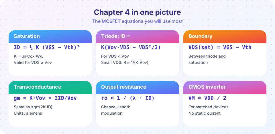
What you will learn
- Which MOSFET equation fits each region and application
- How the chapter's ideas compare with the BJT chapter
- Where you need more practice, from a ten-question quiz
Recap table
| Lesson | Key idea | Formula or rule | Watch out for |
|---|---|---|---|
| Structure and I–V | Gate voltage forms a channel; three regions | Saturation: I_D = ½K·V_ov²; triode: K(V_ov·V_DS − V_DS²/2) | Check V_DS against V_ov; the ½ factor; V_th varies |
| Switch and CMOS | Low R_DS(on); complementary pair has no static path | R_DS(on) ≈ 1/(K·V_ov); P = C·V²·f | Logic-level parts; gate charge; body diode |
| Small-signal model | Open gate, g_m·v_gs source, r_o | g_m = 2I_D/V_ov; A_v = −g_m(R_D ∥ r_o ∥ R_L) | Lower gain than a BJT but huge R_in and better linearity |
BJT and MOSFET side by side
| Question | BJT | MOSFET |
|---|---|---|
| What controls the output current? | Base current / V_BE | Gate voltage V_GS |
| DC input current | I_C/β | About zero |
| Law | I_C = I_s·e^(V_BE/V_T) | I_D = ½K(V_GS − V_th)² |
| g_m | I_C/V_T | 2I_D/V_ov |
| "Saturation" means | Switch fully on | Amplifier region (pinch-off) |
| Switch drop | V_CE(sat) ≈ 0.2 V | I × R_DS(on), can be millivolts |
| Intrinsic gain | V_A/V_T (thousands) | 2/(λ·V_ov) (tens to hundreds) |
Study the "saturation" row twice. The word means different things for the two devices, and mixing them up is one of the most common mistakes.
Common misconceptions
"I_D = K·V_ov² in saturation." With K defined as μ_nC_oxW/L the formula has a factor ½. Some texts absorb the ½, so always check.
"Gate current is zero, so gate drive power is zero." Charging the gate capacitance each cycle costs power, C·V²·f in a fast switch.
"A MOSFET at V_GS = V_th conducts well." At the threshold the current is tiny. A switch needs a gate drive several volts above it.
Try it
First, a comparison table. For a given drain current and overdrive, the program prints g_m, the intrinsic gain and the voltage gain of a common-source stage, so you can see how design choices move the numbers.
Press Run (or Ctrl + Enter) to see the result here.
Program input · what you'd type while the program runs
Type the answers before you press Run, one per line. Each time the program reads a line (with input()), it gets the next line from this box.
Second, an interactive MOSFET region trainer. Change the gate and drain voltages for an NMOS with V_th = 1 V and see which region it is in, plus the formula you would use.
Check your understanding
Quick check · 10 questions
of 10 answered You scored / 10 · perfect!
-
1. An n-channel MOSFET has V_th = 0.8 V and K = 5 mA/V². At V_GS = 1.8 V in saturation, what is I_D?
V_ov = 1 V, so I_D = ½ × 5 mA/V² × 1² = 2.5 mA. -
2. The device above has V_DS = 0.5 V at V_GS = 1.8 V. Which region is it in?
V_DS = 0.5 V is below V_ov = 1 V, so it is in the triode region. -
3. What is R_DS(on) for small V_DS with K = 5 mA/V² and V_ov = 1 V?
R_DS = 1/(K·V_ov) = 1/(0.005 × 1) = 200 Ω. -
4. g_m for I_D = 1 mA and V_ov = 0.2 V is:
g_m = 2I_D/V_ov = 2 mA / 0.2 V = 10 mS. -
5. A CMOS gate with C = 5 pF at V_DD = 1.2 V switching at 2 GHz dissipates about:
P = C·V²·f = 5×10⁻¹² × 1.44 × 2×10⁹ = 14.4 mW. -
6. Why does a CMOS inverter dissipate almost no static power?
In each steady state exactly one of the NMOS and PMOS is off. -
7. A common-source stage has g_m = 4 mS and R_D = 2.5 kΩ with no load. What is A_v?
A_v = −g_m·R_D = −0.004 × 2500 = −10. -
8. What is the main reason a MOSFET amplifier can handle a larger input than a BJT stage for the same distortion?
V_ov is typically a volt or so, much larger than V_T = 25.9 mV in the BJT's distortion formula. -
9. Which statement about the datasheet threshold voltage is correct?
V_th marks the start of conduction. For a switch, check R_DS(on) at your gate voltage. -
10. Intrinsic gain g_m·r_o = 2/(λ·V_ov). Reducing V_ov while keeping I_D (larger W/L) does what to it?
A smaller V_ov raises 2/(λ·V_ov), at the cost of signal swing and linearity.
Summary
- Saturation: I_D = ½K·V_ov² for V_DS ≥ V_ov; triode: I_D = K(V_ov·V_DS − V_DS²/2); R_DS(on) ≈ 1/(K·V_ov).
- Always assume a region, solve, then check V_DS against V_ov.
- A MOSFET switch has very low loss; the CMOS inverter has no static power and P = C·V²·f dynamic power.
- Small signal: g_m = 2I_D/V_ov, r_o = 1/(λI_D), A_v = −g_m(R_D ∥ r_o ∥ R_L), with a huge input resistance.
- You now have the two transistor families and the tools to bias, switch and model them. The next chapters turn them into amplifiers, op amps, filters and power supplies.
Next: back to the Analog Electronics course page
Track your progress
Create a free account to tick off lessons and pick up where you left off on any device.
of Analog Electronics lessons completed