


















Lesson 12 of 46 · Bipolar Transistors
How a BJT works: structure, equations and regions
Understand how an NPN transistor works, use IC = beta times IB and the exponential law, identify cutoff, active and saturation, and find a Q point on the load line.
Why should a thin slice of p-type silicon between two n-type regions amplify current? The answer is a short story about electrons: they are injected from the emitter, race across the base so fast that nearly all of them are swept into the collector, and only a few are lost on the way. Those few are the base current. Once you see this picture, the equations (I_C = βI_B, the exponential law, the three regions) stop being rules to memorize and become consequences you can derive.
This lesson builds the physical picture, gives the equations, plots the output characteristics, and uses a load line to find where a transistor sits in a real circuit.
What you will learn
- How the emitter, base and collector layers make current gain possible
- The relations I_E = I_C + I_B, I_C = βI_B, α = β/(β+1) and the exponential law
- The three regions of operation and how to recognize each from voltages
- The Early effect and the output characteristic curves
- How to find the Q point with a load line, and why fixed bias is fragile
Key terms
Active region: the amplifier region, with the base-emitter junction forward biased and the base-collector junction reverse biased.
Saturation: both junctions forward biased; the transistor acts like a closed switch with V_CE of about 0.1 to 0.3 V.
Cutoff: both junctions off; almost no collector current.
Early effect: the slight rise of I_C with V_CE in the active region, characterized by the Early voltage V_A.
Q point (quiescent point): the DC operating point (I_C, V_CE) with no signal.
How the current gain arises
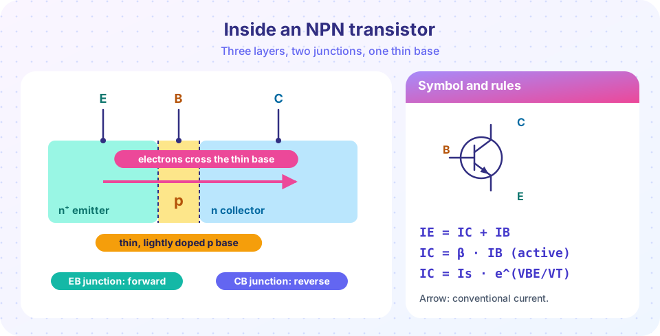
Look at the figure. The emitter is heavily doped n-type (n⁺), so it has many free electrons. A forward bias of about 0.7 V across the emitter-base junction lowers the barrier and the emitter injects electrons into the base. The base is p-type, very thin (a micron or less) and lightly doped, so there are few holes for the electrons to recombine with. The injected electrons are the minority carriers in the base and diffuse toward the collector junction. That junction is reverse biased, so any electron that reaches its edge is swept across by the strong field into the collector.
A small fraction recombine with holes in the base. The holes consumed must be replaced from the base terminal: this is the base current, typically a hundredth of the collector current. A thin, lightly doped base and a heavily doped emitter make that fraction small. The ratio is the current gain β = I_C/I_B.
Kirchhoff's current law for the whole transistor gives the emitter current:
IE = IC + IB
IC = β · IB        IE = (β + 1) · IB
α = IC / IE = β / (β + 1)
With β = 100, α = 0.990: 99 % of the emitter current reaches the collector.
The exponential law
The base-emitter junction is a forward-biased diode, so the collector current follows the diode law:
IC = Is · e^(VBE / VT) VT ≈ 25.9 mV at 300 K
The saturation current I_s depends on the transistor's geometry and temperature, so two "identical" transistors can differ by a large factor at the same V_BE. This law has the same consequences as the diode: V_BE sits near 0.65 to 0.75 V for milliamps of current, rises 60 mV for ten times the current, and falls about 2 mV per °C. In practice you design circuits so that β and I_s hardly matter.
The two viewpoints agree. The base current is I_B = I_C/β, so the voltage V_BE controls the collector current and the current gain is a bookkeeping device for the small input current.
The three regions
| Region | Junctions | Typical voltages (NPN) | Behavior |
|---|---|---|---|
| Cutoff | Both reverse or off | V_BE below about 0.5 V | I_C ≈ 0; open switch |
| Active | BE forward, BC reverse | V_BE ≈ 0.7 V, V_CE above about 0.3 V | I_C = βI_B; amplifier |
| Saturation | Both forward | V_BE ≈ 0.75 V, V_CE ≈ 0.1 to 0.3 V | I_C set by the circuit, less than βI_B; closed switch |
To decide the region, assume active, calculate, then check: V_CE must be larger than about 0.2 V (otherwise it is saturated) and I_B must be positive (otherwise it is cut off).
Output characteristics
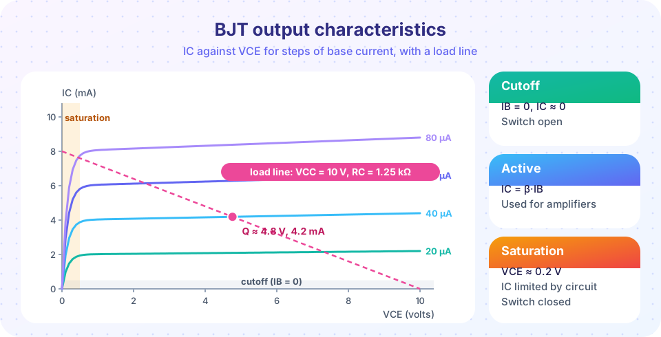
Plot I_C against V_CE for several values of I_B and you get a family of curves like the figure. Each curve rises steeply (saturation) and then flattens (active region). The curves are not perfectly flat: they slope upward slightly because a larger V_CE widens the collector depletion region and narrows the base, slightly increasing the gain. This is the Early effect, named after James Early. Extending the active-region lines backward, they meet the voltage axis at −V_A, where V_A (the Early voltage) is typically 50 to 200 V. The slope corresponds to an output resistance
ro = VA / IC
For V_A = 100 V and I_C = 4 mA this is 25 kΩ. In many hand calculations it is ignored; it limits the maximum gain of an amplifier stage (chapter 5).
The load line and Q point
Put a collector resistor R_C between a supply V_CC and the collector. KVL gives V_CE = V_CC − I_C·R_C. On the graph this is a straight line from (V_CE = V_CC, I_C = 0) to (V_CE = 0, I_C = V_CC/R_C), the load line. The transistor can only operate at a point on both the load line and one of its curves. With V_CC = 10 V, R_C = 1.25 kΩ and I_B = 40 µA, the line crosses the 40 µA curve at about V_CE = 4.8 V, I_C = 4.2 mA (the active-region slope lifts the current slightly above the ideal 4 mA).
Using only the ideal equations: I_C = β·I_B = 100 × 40 µA = 4 mA, V_CE = 10 − 4 mA × 1.25 kΩ = 5.0 V. The check passes (5 V is much more than 0.2 V), so the active-region assumption was right.
Fixed bias is fragile
How do you supply that 40 µA? The easiest way is a base resistor to V_CC: R_B = (10 − 0.7)/40 µA = 232.5 kΩ. This is called fixed bias, and it has a serious flaw: I_B is fixed by R_B, so I_C = β·I_B is proportional to β, and β varies. Try β from 50 to 200:
| β | I_C | V_CE = 10 − 1.25k·I_C | Region |
|---|---|---|---|
| 50 | 2 mA | 7.5 V | active |
| 100 | 4 mA | 5.0 V | active |
| 150 | 6 mA | 2.5 V | active |
| 200 | 8 mA | 0 V (calculated) | saturated |
A transistor with β = 200 would saturate and distort any signal. Chapter 5 shows how emitter resistors and voltage dividers make the Q point nearly independent of β. For switching (lesson 3) the problem goes away because we saturate deliberately.
Common misconceptions
"β is a constant of the transistor." It changes with part, current, temperature and V_CE. Datasheets give ranges such as 100 to 300.
"V_BE controls current linearly." It is exponential: a few tens of millivolts change the current by a large factor.
"In saturation I_C = βI_B." In saturation the collector current is limited by the external circuit, and I_C is less than βI_B.
Try it
First, reproduce the output characteristics and load line. Change V_CC, R_C or the base-current steps, and see how the Q point moves.
Press Run (or Ctrl + Enter) to see the result here.
Program input · what you'd type while the program runs
Type the answers before you press Run, one per line. Each time the program reads a line (with input()), it gets the next line from this box.
Second, the fixed-bias circuit with realistic spread in β. The chart shows how V_CE collapses as β rises, and where the transistor saturates.
Press Run (or Ctrl + Enter) to see the result here.
Program input · what you'd type while the program runs
Type the answers before you press Run, one per line. Each time the program reads a line (with input()), it gets the next line from this box.
Check your understanding
Quick check · 6 questions
of 6 answered You scored / 6 · perfect!
-
1. An NPN transistor has β = 120 and I_C = 6 mA in the active region. What is the base current?
I_B = I_C/β = 6 mA / 120 = 50 µA. -
2. With β = 100, what is α = I_C/I_E?
α = β/(β+1) = 100/101 = 0.990. -
3. What happens to V_BE (at fixed collector current) when a transistor warms up?
As with a diode, V_BE falls about 2 mV per °C at constant current. -
4. A transistor in a circuit with V_CE = 0.15 V and a large base current is in which region?
A very small V_CE with both junctions forward biased is saturation. -
5. What does the Early effect cause?
The base narrows as V_CE rises, so the collector current increases slightly and the output curves slope upward. -
6. Why is fixed bias a poor choice for an amplifier?
With I_B fixed by R_B, I_C = βI_B moves with β, shifting the Q point.
Summary
- A heavily doped emitter injects electrons into a thin base; most are collected, giving I_C = βI_B and I_E = I_C + I_B.
- The exponential law I_C = I_s·e^(V_BE/V_T) shows V_BE near 0.7 V and a −2 mV/°C drift.
- Regions: cutoff (off), active (amplifier), saturation (V_CE ≈ 0.2 V, I_C below βI_B).
- The Early effect gives r_o = V_A/I_C. The load line V_CE = V_CC − I_CR_C finds the Q point.
- Fixed bias depends on β and is fragile; better bias circuits come in chapter 5.
Next: The BJT as a switch
Track your progress
Create a free account to tick off lessons and pick up where you left off on any device.
of Analog Electronics lessons completed