


















Lesson 18 of 46 · MOSFETs
The MOSFET as a switch and the CMOS inverter
Use a MOSFET as a low-loss switch, size the gate drive, then see how a PMOS and NMOS pair make the CMOS inverter and why chips spend power only when switching.
A MOSFET is nearly the perfect switch. Off, it carries almost no current. On, it is a small resistor, often well under an ohm and in power devices a few milliohms, so it drops very little voltage and wastes very little power. The gate draws no steady current, so a tiny signal can control a large load. Combine one NMOS and one PMOS and you get the CMOS inverter, the building block of every digital chip, which consumes almost no power when its output is not changing.
This lesson covers both: switching real loads with a single MOSFET, and the complementary pair that underlies logic.
What you will learn
- How to use an NMOS as a low-side switch and calculate its losses
- What R_DS(on), logic-level MOSFETs and the body diode are
- How gate charge limits switching speed and what a gate resistor does
- How the CMOS inverter works and why its static power is almost zero
- How to estimate dynamic power with P = C·V²·f
Key terms
R_DS(on): the on-resistance between drain and source for a given gate voltage, from the datasheet.
Logic-level MOSFET: one that is fully on at a V_GS of 4.5 V or even 2.5 V, so it can be driven directly from logic.
Gate charge (Q_g): the charge needed to switch the gate fully on; it sets the drive current and switching time.
Body diode: the p-n junction between source and drain that is part of every power MOSFET.
Dynamic power: the power used to charge and discharge capacitances each time a CMOS gate switches.
The MOSFET switch
Put the load between the supply and the drain, and connect the source to ground (a low-side switch, just like the BJT switch). With V_GS = 0 the channel is absent and the load is off. Raise V_GS well above V_th and the transistor enters the triode region with a tiny V_DS, behaving like a resistor
RDS(on) ≈ 1 / ( K · Vov )
For our teaching transistor (K = 2 mA/V²) with V_GS = 5 V, V_ov = 4 V and R_DS(on) = 125 Ω, which is large because this transistor is tiny. A power MOSFET has a huge W/L ratio (thousands of cells in parallel) and R_DS(on) can be 10 mΩ or less. Switching a 2 A, 12 V motor with a 20 mΩ device drops 40 mV and dissipates P = I²R = 4 × 0.02 = 80 mW. A BJT in saturation passing the same current would drop 0.2 V and dissipate 0.4 W, and would need base drive of about 200 mA at a forced β of 10. The MOSFET is far more efficient at high current.
Choosing the part
- Gate threshold versus drive voltage. The datasheet R_DS(on) is quoted at a specific V_GS (such as 10 V or 4.5 V). A standard MOSFET needs about 10 V to be fully on, so a 5 V logic pin will not drive it properly. A logic-level MOSFET is rated at 4.5 V (and some at 2.5 V) and works from a microcontroller. The V_th in the datasheet is only where the channel starts to form, for example at 250 µA. It says nothing about how well the device conducts at full load.
- Voltage and current ratings. V_DS(max) must exceed the supply with margin (including inductive spikes) and the current rating must be met at your temperature.
- Gate voltage limit. V_GS(max) is typically ±20 V; exceeding it destroys the oxide.
Gate drive
The gate is a capacitor (C_iss of hundreds of picofarads to nanofarads). Turning the switch on means delivering the gate charge Q_g; the switching time is roughly t = Q_g / I_gate. With Q_g = 20 nC and a 100 mA driver, t ≈ 200 ns. A logic pin that can only supply 10 mA takes 2 µs, during which the MOSFET sits in its intermediate, high-dissipation state. For fast switching, use a gate-driver chip. A series gate resistor (10 to 100 Ω) slows the edges deliberately to reduce ringing and electromagnetic noise, and a pull-down resistor (10 kΩ to 100 kΩ from gate to source) keeps the gate low if the driver is disconnected or floating.
The body diode
Every power MOSFET contains a diode from source to drain (for an NMOS: the p-type body to the n-type drain). It conducts when the drain is more negative than the source. It acts as a flyback diode for inductive loads (though a separate fast diode is often better) and is essential in bridge circuits that drive motors in both directions. In some circuits it is a hazard: a MOSFET cannot block current in the reverse direction.
The CMOS inverter
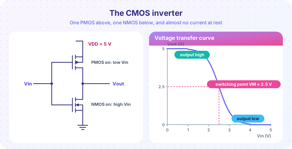
Now take the figure. A PMOS transistor sits between V_DD and the output; an NMOS sits between the output and ground. Their gates are joined to the input.
- Input low (0 V). The NMOS has V_GS = 0 and is off. The PMOS has its gate 5 V below its source, so it is on. The output is connected to V_DD: output high.
- Input high (V_DD). The NMOS is on and the PMOS is off. The output is connected to ground: output low.
In either steady state, one transistor is off, so there is no DC path from supply to ground and the supply current is only leakage. That is why CMOS dominates digital design: billions of gates sit idle at nearly zero power.
The transfer curve
Between the two states, both transistors briefly conduct. Near the switching threshold V_M, both are in saturation and the gain is very large (dozens to hundreds, limited by r_o), so the output falls steeply, as in the figure. For matched transistors (equal K and equal threshold magnitudes) the switching point sits at about V_DD/2. This steep, symmetrical curve regenerates logic levels: a slightly degraded input still produces a clean 0 or 1. A brief burst of shoot-through current flows from the supply to ground when the input is near V_M.
Dynamic power
When the output switches, the load capacitance C (the wiring and the gates it drives) must be charged or discharged. Each full cycle takes C·V_DD² of energy from the supply: half is lost as heat while the capacitor charges, and the other half, stored on it, is lost as heat when it discharges. So the average power for a gate switching at frequency f is about
P = C · VDD² · f
For C = 10 pF, V_DD = 3.3 V and f = 100 MHz: P = 10 × 10⁻¹² × 10.89 × 10⁸ = 10.9 mW. The V² term explains why chip designers keep lowering the supply voltage: at 1.0 V the same load costs 1.0 mW, almost eleven times less.
Common misconceptions
"A MOSFET has no gate current, so any pin can drive it." The steady current is zero, but the gate must be charged each time. A weak driver switches a big MOSFET slowly and it overheats in the middle of the transition.
"The datasheet V_th means the MOSFET is on." It is only where conduction begins. Check R_DS(on) at your actual gate voltage.
"CMOS uses no power." The static power is tiny, but the dynamic power C·V²·f is the main power consumer in processors.
Try it
First, the inverter's transfer curve from the square-law equations. For each input voltage the program finds the output where the NMOS and PMOS currents are equal. Try making the PMOS stronger or weaker (change Kp) and watch the switching point move.
Press Run (or Ctrl + Enter) to see the result here.
Program input · what you'd type while the program runs
Type the answers before you press Run, one per line. Each time the program reads a line (with input()), it gets the next line from this box.
Second, dynamic power. Plot P = C·V²·f for a gate load of 10 pF across frequencies, for three supply voltages, and read off the savings from a lower voltage.
Press Run (or Ctrl + Enter) to see the result here.
Program input · what you'd type while the program runs
Type the answers before you press Run, one per line. Each time the program reads a line (with input()), it gets the next line from this box.
Check your understanding
Quick check · 5 questions
of 5 answered You scored / 5 · perfect!
-
1. A MOSFET has R_DS(on) = 25 mΩ and carries 4 A. What is the power dissipated in it?
P = I²R = 16 × 0.025 = 0.4 W. -
2. Why does a CMOS inverter use almost no power when its input is steady?
At a steady input one transistor is off, so only leakage current flows. -
3. A gate has C = 20 pF, V_DD = 2 V and f = 50 MHz. What is the dynamic power?
P = C·V²·f = 20×10⁻¹² × 4 × 50×10⁶ = 4 mW. -
4. Which is the best sign that a MOSFET can be driven from a 3.3 V microcontroller pin?
R_DS(on) specified at a low V_GS means it is fully on at that gate voltage (a logic-level part). -
5. Why add a pull-down resistor from gate to source?
A floating gate can pick up charge and turn the MOSFET on unpredictably.
Summary
- A MOSFET switch has R_DS(on) = 1/(K·V_ov) in the simple model and very low loss: P = I²R_DS(on).
- Use a logic-level part for microcontroller drive; check R_DS(on) at your actual V_GS.
- Gate charge Q_g sets switching time; add a gate resistor and a pull-down resistor.
- The body diode conducts from source to drain and matters in bridges and with inductive loads.
- In a CMOS inverter one transistor is always off at steady state; the switching point is about V_DD/2.
- Dynamic power is P = C·V_DD²·f, so a lower supply voltage saves a great deal.
Track your progress
Create a free account to tick off lessons and pick up where you left off on any device.
of Analog Electronics lessons completed