


















Lesson 23 of 46 · Amplifier Basics and Biasing
Biasing a bipolar transistor
Learn why a transistor needs bias, how a DC load line locates the Q-point, and how to design a stable voltage-divider bias with worked numbers.
A bipolar transistor is a current amplifier: a small base current IB controls a larger collector current IC = β · IB. But that only works while the transistor sits in its active region, where the base-emitter junction is forward biased by about 0.7 V and the collector-base junction is reverse biased. If you simply connect a signal to the base with nothing else, the negative half of the wave switches the transistor off and the output is badly distorted.
Biasing is the art of adding resistors and a supply so the transistor rests in the middle of its active region with no signal, then lets the signal swing up and down around that resting point. This lesson shows how to choose the resting point, how to see it on a load line, and why one particular arrangement, voltage-divider bias, is used in almost every discrete amplifier.
What you will learn
- Explain what the Q-point is and why it should be near the middle of the load line.
- Draw a DC load line and read the Q-point from it.
- Design a voltage-divider bias network in four steps.
- Explain why divider bias with an emitter resistor is stable when β varies.
Key terms
Q-point (quiescent point): the DC values IC and VCE with no input signal applied.
Load line: the straight line on the IC-VCE graph that shows every combination the external circuit allows.
Active region: the region where IC ≈ β · IB and VCE is above about 0.2 V.
Thermal runaway: a self-reinforcing rise of current and temperature that can destroy a transistor.
Stiff divider: a base divider whose current is much larger than the base current, so the base voltage hardly depends on β.
The DC load line
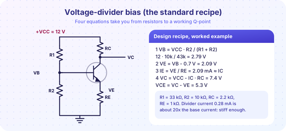
Take the circuit in the picture with VCC = 12 V. Around the collector-emitter loop, Kirchhoff's voltage law gives
VCC = IC · RC + VCE + IE · RE
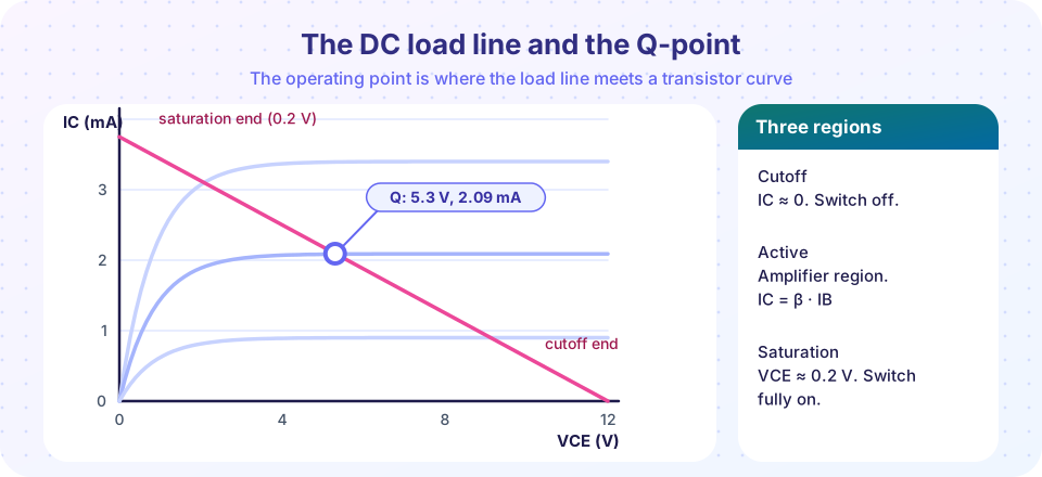
Because IE ≈ IC for any decent β, this becomes VCE = VCC - IC · (RC + RE), a straight line. Two points draw it:
- Cutoff end:
IC = 0,VCE = VCC = 12 V. - Saturation end:
VCE ≈ 0,IC = VCC / (RC + RE) = 12 / 3.2 kΩ = 3.75 mA.
The transistor can only operate at a point on this line. Where exactly depends on the base current. A good bias puts the Q-point near the middle, around VCE ≈ VCC / 2, so the output can swing equally far up and down before it clips.
Why simple fixed bias fails
The easiest idea is one resistor RB from VCC to the base. Then IB = (VCC - 0.7) / RB and IC = β · IB. The trouble is that β is not a reliable number. A datasheet may say "100 to 300" for the same part number, and β also rises with temperature. With RB = 800 kΩ, IB = 14.1 µA, and IC becomes 1.06 mA at β = 75, 2.1 mA at β = 150 and 4.2 mA at β = 300. The same circuit is cutoff-ish in one case and nearly saturated in the next. Worse, a hotter transistor conducts more, heats more, and conducts more again: thermal runaway.
Voltage-divider bias with an emitter resistor
The fix is negative feedback. Let resistors R1 and R2 hold the base at a roughly fixed voltage VB. The emitter sits one diode drop below that, VE = VB - 0.7 V, and the emitter resistor converts it to a current IE = VE / RE. Notice that β does not appear. If β rises and IC tries to grow, VE rises, VBE shrinks, and the transistor throttles itself back.
The four-step design recipe
VB = VCC · R2 / (R1 + R2)(treating the divider as unloaded)VE = VB - 0.7 VIE = VE / RE ≈ ICVC = VCC - IC · RCandVCE = VC - VE
Worked example. VCC = 12 V, R1 = 33 kΩ, R2 = 10 kΩ, RC = 2.2 kΩ, RE = 1 kΩ.
VB = 12 × 10 / 43 = 2.79 VVE = 2.09 VIE = 2.09 mAVC = 12 - 2.09 mA × 2.2 kΩ = 7.4 V, soVCE = 7.4 - 2.09 = 5.3 V
VCE = 5.3 V is close to half of 12 V: a good Q-point.
A more exact answer
Step 1 ignored the current drawn by the base. The accurate version replaces the divider with its Thevenin equivalent, VTH = 2.79 V and RTH = R1 ∥ R2 = 7.67 kΩ, and gives
IB = (VTH - 0.7) / (RTH + (β + 1) · RE)
With β = 150 this yields IB = 13.2 µA, IC = 1.98 mA and VCE = 5.6 V, within 5% of the quick estimate. That is the point of a stiff divider: the divider current (12 V / 43 kΩ = 0.28 mA) is about 20 times the base current, so the shortcut is accurate.
The stability test
Run the exact formula for β = 75, 150 and 300 and IC only moves between 1.87 mA and 2.03 mA. Compare that with the fixed-bias circuit, where IC varied by a factor of four. You trade some emitter signal gain for this stability, and you will recover the gain with a bypass capacitor in the next lesson.
Rules of thumb for choosing values
- Choose
VEof about 1-2 V (a tenth of the supply is typical): enough drop acrossREfor good thermal stability without wasting headroom. - Choose the divider current at
10 × IBor more. - Aim for
VCE ≈ VCC / 2unless you know the output swing needed. - Check that
ICstays below the transistor's maximum rating, and thatVCE · ICstays below its power rating.
Common misconceptions
"β is a fixed number I can design with." It varies widely between units and with temperature; good bias is designed so the result barely depends on it.
"The Q-point should be where gain is highest." It should be where the swing is largest and distortion smallest, usually the middle of the load line.
"A 0.7 V drop is exact." VBE is about 0.6-0.7 V for small silicon transistors and falls about 2 mV per degree Celsius of warming.
Try it
The first example is a solver. It compares fixed bias and divider bias across a range of β values, using the exact formulas above. It is a calculator for the DC circuit, not a full transistor model.
Press Run (or Ctrl + Enter) to see the result here.
Program input · what you'd type while the program runs
Type the answers before you press Run, one per line. Each time the program reads a line (with input()), it gets the next line from this box.
The second example draws the load line and Q-point for your own resistor values. Edit R1, R2, RC and RE and run it again. It uses the exact divider formula and assumes β = 150.
Press Run (or Ctrl + Enter) to see the result here.
Program input · what you'd type while the program runs
Type the answers before you press Run, one per line. Each time the program reads a line (with input()), it gets the next line from this box.
The third example is an interactive bias explorer with sliders. It tells you whether the transistor is in cutoff, the active region or saturation.
Check your understanding
Quick check · 5 questions
of 5 answered You scored / 5 · perfect!
-
1. What does the Q-point describe?
Q stands for quiescent, meaning resting. It is the DC operating point before any signal arrives. -
2. For VCC = 12 V, RC = 2.2 kΩ and RE = 1 kΩ, what collector current does the saturation end of the load line show?
IC(sat) = VCC / (RC + RE) = 12 V / 3.2 kΩ = 3.75 mA. -
3. Why is divider bias with an emitter resistor stable when β changes?
The base voltage is fixed by the stiff divider, so a rising emitter voltage reduces VBE and throttles the current. -
4. A divider uses R1 = 47 kΩ and R2 = 10 kΩ from 12 V. What is the unloaded base voltage?
VB = 12 × 10 / 57 = 2.1 V. -
5. Where should the Q-point usually sit for the largest symmetrical output swing?
From the middle the output can move equally far toward cutoff and toward saturation before clipping.
Summary
- Bias sets the DC Q-point so the transistor stays active while the signal swings.
- The load line
VCE = VCC - IC(RC + RE)shows every allowed operating point. - Fixed bias depends strongly on β; voltage-divider bias with
REdoes not. - Design in four steps:
VB,VE = VB - 0.7,IE = VE / RE,VCandVCE; aim forVCE ≈ VCC / 2.
Track your progress
Create a free account to tick off lessons and pick up where you left off on any device.
of Analog Electronics lessons completed